
Data Sheet


MFRC522 All information provided in this document is subject to legal disclaimers. © NXP Semiconductors N.V. 2016. All rights reserved.
Product data sheet
COMPANY PUBLIC
Rev. 3.9 — 27 April 2016
112139 16 of 95
NXP Semiconductors
MFRC522
Standard performance MIFARE and NTAG frontend
8.1.4 I
2
C-bus interface
An I
2
C-bus (Inter-IC) interface is supported to enable a low-cost, low pin count serial bus
interface to the host. The I
2
C-bus interface is implemented according to
NXP Semiconductors’ I
2
C-bus interface specification, rev. 2.1, January 2000. The
interface can only act in Slave mode. Therefore the MFRC522 does not implement clock
generation or access arbitration.
The MFRC522 can act either as a slave receiver or slave transmitter in Standard mode,
Fast mode and High-speed mode.
SDA is a bidirectional line connected to a positive supply voltage using a current source or
a pull-up resistor. Both SDA and SCL lines are set HIGH when data is not transmitted. The
MFRC522 has a 3-state output stage to perform the wired-AND function. Data on the
I
2
C-bus can be transferred at data rates of up to 100 kBd in Standard mode, up to
400 kBd in Fast mode or up to 3.4 Mbit/s in High-speed mode.
If the I
2
C-bus interface is selected, spike suppression is activated on lines SCL and SDA
as defined in the I
2
C-bus interface specification.
See Table 155 on page 79
for timing requirements.
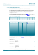
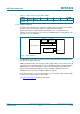
Table 14. Address byte 0 register; address MOSI
7 (MSB) 6 5 4 3 2 1 0 (LSB)
1 = read
0 = write
reserved address
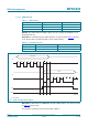
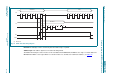
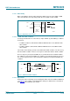
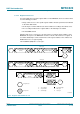
Fig 11. I
2
C-bus interface
001aak590
MFRC522
SDA
SCL
I2C
EA
ADR_[5:0]
PULL-UP
NETWORK
CONFIGURATION
WIRING
PULL-UP
NETWORK
MICROCONTROLLER