
Data Sheet


xxxxxxxxxxxxxxxxxxxxx xxxxxxxxxxxxxxxxxxxxxxxxxx xxxxxxx x x x xxxxxxxxxxxxxxxxxxxxxxxxxxxxxx xxxxxxxxxxxxxxxxxxx xx xx xxxxx
xxxxxxxxxxxxxxxxxxxxxxxxxxx xxxxxxxxxxxxxxxxxxx xxxxxx xxxxxxxxxxxxxxxxxxxxxxxxxxxxxxxxxxx xxxxxxxxxxxx x x
xxxxxxxxxxxxxxxxxxxxx xxxxxxxxxxxxxxxxxxxxxxxxxxxxxx xxxxx xxxxxxxxxxxxxxxxxxxxxxxxxxxxxxxxxxxxxxxxxxxxxxxxxx xxxxxxxx
xxxxxxxxxxxxxxxxxxxxxxxxx xxxxxxxxxxxxxxxxxxxx xxx
MFRC522 All information provided in this document is subject to legal disclaimers. © NXP Semiconductors N.V. 2016. All rights reserved.
Product data sheet
COMPANY PUBLIC
Rev. 3.9 — 27 April 2016
112139 15 of 95
NXP Semiconductors
MFRC522
Standard performance MIFARE and NTAG frontend
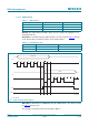
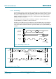
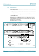
Remark: The data byte can be sent directly after the address byte on pin RX.
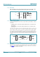
Address byte: The address byte has to meet the following format:
The MSB of the first byte sets the mode used. To read data from the MFRC522, the MSB is set to logic 1. To write data to the
MFRC522 the MSB is set to logic 0. Bit 6 is reserved for future use, and bits 5 to 0 define the address; see Table 14
.
(1) Reserved.
Fig 10. UART write data timing diagram
001aak589
SA
ADDRESS
RX
TX
MX
DTRQ
A0 A1 A2 A3 A4 A5 (1) SO SA D0 D1 D2 D3 D4 D5 D6 D7 SO
SA A0 A1 A2 A3 A4 A5 (1) SO
DATA
ADDRESS
R/W
R/W