
Data Sheet


MFRC522 All information provided in this document is subject to legal disclaimers. © NXP Semiconductors N.V. 2016. All rights reserved.
Product data sheet
COMPANY PUBLIC
Rev. 3.9 — 27 April 2016
112139 13 of 95
NXP Semiconductors
MFRC522
Standard performance MIFARE and NTAG frontend
8.1.3.3 UART framing
Remark: The LSB for data and address bytes must be sent first. No parity bit is used
during transmission.
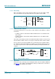
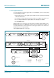
Read data: To read data using the UART interface, the flow shown in Table 12
must be
used. The first byte sent defines both the mode and the address.
Write data: To write data to the MFRC522 using the UART interface, the structure shown
in Table 13
must be used.
The first byte sent defines both the mode and the address.
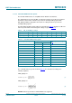
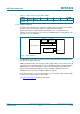
Table 11. UART framing
Bit Length Value
Start 1-bit 0
Data 8 bits data
Stop 1-bit 1
Table 12. Read data byte order
Pin Byte 0 Byte 1
RX (pin 24) address -
TX (pin 31) - data 0
(1) Reserved.
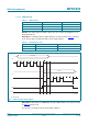
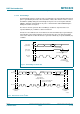
Fig 9. UART read data timing diagram
001aak588
SA
ADDRESS
RX
TX
MX
DTRQ
A0 A1 A2 A3 A4 A5
(1)
SO
SA D0 D1 D2 D3 D4 D5 D6 D7 SO
DATA
R/W