
Data Sheet


Revision 2.0 Page 70 of 74
nRF24L01 Product Specification
PCB layout examples
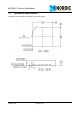
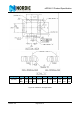
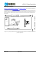
Figure 31. on page 70, Figure 32. on page 71 and Figure 33. on page 71 show a PCB layout example for
the application schematic in Figure 30. on page 69
.
A double-sided FR-4 board of 1.6mm thickness is used. This PCB has a ground plane on the bottom layer.
Additionally, there are ground areas on the component side of the board to ensure sufficient grounding of
critical components. A large number of via holes connect the top layer ground areas to the bottom layer
ground plane.
Figure 31. Top overlay (nRF24L01 RF layout with single ended connection to PCB antenna and 0402 size
passive components)