
Data Sheet

Revision 2.0 Page 45 of 74
nRF24L01 Product Specification
8 Data and Control Interface
The data and control interface gives you access to all the features in the nRF24L01. The data and control
interface consists of the following six 5Volt tolerant digital signals:
• IRQ (this signal is active low and is controlled by three maskable interrupt sources)
• CE (this signal is active high and is used to activate the chip in RX or TX mode)
• CSN (SPI signal)
• SCK (SPI signal)
• MOSI (SPI signal)
• MISO (SPI signal)
You can use the SPI to activate the nRF24L01 data FIFOs or the register map by 1 byte SPI commands
during all modes of operation.
8.1 Features
• Special SPI commands for quick access to the most frequently used features
• 0-8Mbps 4-wire SPI serial interface
• 8 bit command set
• Easily configurable register map
• Full three level FIFO for both TX and RX direction
8.2 Functional description
The SPI is a standard SPI with a maximum data rate of 8Mbps.
8.3 SPI operation
This chapter describes the SPI commands and SPI timing.
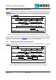
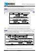
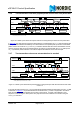
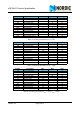
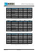
8.3.1 SPI Commands
The SPI commands are shown in Table 16.. Every new command must be started by a high to low transi-
tion on CSN.
In parallel to the SPI command word applied on the MOSI pin, the STATUS register is shifted serially out on
the MISO pin.
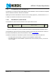
The serial shifting SPI commands is in the following format:
<Command word: MSBit to LSBit (one byte)>
<Data bytes: LSByte to MSByte, MSBit in each byte first>
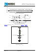
See Figure 23. on page 47
and Figure 24. on page 48 for timing information.