
Data Sheet

Revision 2.0 Page 20 of 74
nRF24L01 Product Specification
.
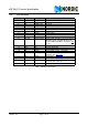
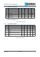
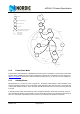
Figure 3. Radio control state diagram
6.1.2 Power Down Mode
In power down mode nRF24L01 is disabled with minimal current consumption. In power down mode all the
register values available from the SPI are maintained and the SPI can be activated. For start up time see
Table 13. on page 22
. Power down mode is entered by setting the PWR_UP bit in the CONFIG register low.
6.1.3 Standby Modes
By settting the PWR_UP bit in the CONFIG register to 1, the device enters standby-I mode. Standby-I mode
is used to minimize average current consumption while maintaining short start up times. In this mode part
of the crystal oscillator is active. This is the mode the nRF24L01 returns to from TX or RX mode when CE
is set low.
In standby-II mode extra clock buffers are active compared to standby-I mode and much more current is
used compared to standby-I mode. Standby-II occurs when CE is held high on a PTX device with empty TX
FIFO. If a new packet is uploaded to the TX FIFO, the PLL starts and the packet is transmitted.
VDD >= 1.9V
Undefined
Power on
reset
10.3ms
Power Down
Standby-I
RX Mode
TX Mode
Standby-II
RX Settling
130 us
Start up
1.5ms
PWR_UP = 1
PWR_UP = 0
TX Settling
130 us
TX FIFO not empty
PRIM_RX = 0
CE = 1 for more than 10µs
PRIM_RX = 1
CE = 1
CE = 0
TX FIFO empty
CE = 1
TX FIFO not empty
CE = 1
PRIM_RX = 0
TX FIFO empty
CE = 1
PWR_UP = 0
PWR_UP = 0
PWR_UP=0
CE = 0
PWR_UP=0
PWR_UP=0
TX finished with one packet
CE = 0
CE = 1
TX FIFO not empty
Possible operating mode
Recommended path between operating modes
Possible path between operating modes
Recommended operating mode
Transition state
CE = 1
Pin signal condition
PWR_DN = 1
Bit state condition
Undefined
TX FIFO empty
System information
Undefined
Legend: