
Data Sheet

Revision 2.0 Page 18 of 74
nRF24L01 Product Specification
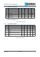
5.6 DC characteristics
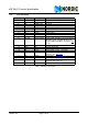
Table 9. Digital input pin
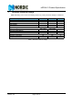
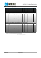
Table 10. Digital output pin
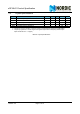
5.7 Power on reset
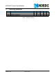
Table 11. Power on reset
Symbol Parameter (condition) Notes Min. Typ. Max. Units
V
IH
HIGH level input voltage 0.7VDD
5.25
a
a. If the input signal >3.6V, the VDD of the nRF24L01 must be between 2.7V and 3.3V (3.0V±10%)
V
V
IL
LOW level input voltage VSS 0.3VDD V
Symbol Parameter (condition) Notes Min. Typ. Max. Units
V
OH
HIGH level output voltage (I
OH
=-0.25mA) VDD -0.3 VDD V
V
OL
LOW level output voltage (I
OL
=0.25mA) 0.3 V
Symbol Parameter (condition) Notes Min. Typ. Max. Units
T
PUP
Power ramp up time
a
a. From 0V to 1.9V
100 ms
T
POR
Power on reset
b
b. Measured when the VDD reaches 1.9V to when the reset finishes
1.6 5.3 10.3 ms