
Specifications

SPECIFICASPECIFICA
SPECIFICASPECIFICA
SPECIFICA
TIONS AND BUFFER OPTIONSTIONS AND BUFFER OPTIONS
TIONS AND BUFFER OPTIONSTIONS AND BUFFER OPTIONS
TIONS AND BUFFER OPTIONS
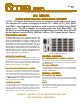
DX/256x256 SERIES MADX/256x256 SERIES MA
DX/256x256 SERIES MADX/256x256 SERIES MA
DX/256x256 SERIES MA
TRIXTRIX
TRIXTRIX
TRIX
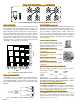
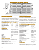
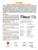
DX/256x256 Mainframe Rear View with IEEE488 and RS232 Control
INPUT and OUTPUT BUFFERSINPUT and OUTPUT BUFFERS
INPUT and OUTPUT BUFFERSINPUT and OUTPUT BUFFERS
INPUT and OUTPUT BUFFERS
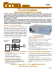
Optional Input and/or output buffer modules convert the system to
RS-422 and/or RS-232 levels. Each buffer module has sixty-four
(64) channels so a fully buffered 256x256 system has four input
buffers and four output buffers. When these modules are used,
the specifications of the system are determined by the input and/
or output buffers present.
The RS-422 input and output buffer modules have two options for
connectors, 68 pin male header or 78 pin female "D" connector.
RS-422 Input Buffer Characteristic:
Common Mode Input Voltage (Vcm) -7V<Vcm<+7V
Differential Voltage Swing 200 mV Min
Input Resistance 6.8 KOhm Typical
Data Rate 20 Mb/s Max
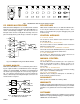
Fig. 2
TX-2
The DX Series is intended to switch almost any digital stream
data stream in a nonblocking (any input to any output without
disturbing previously set paths), full fan out (any one input to any
or all outputs) configurations. The Basic system is intended to
switch TTL or CMOS signal levels.
When used without buffer modules, the system conforms to all
TTL/LVTTL specifications below
DX SPECIFICADX SPECIFICA
DX SPECIFICADX SPECIFICA
DX SPECIFICA
TIONS (signal w/o buffers)TIONS (signal w/o buffers)
TIONS (signal w/o buffers)TIONS (signal w/o buffers)
TIONS (signal w/o buffers)
DX SPECIFICADX SPECIFICA
DX SPECIFICADX SPECIFICA
DX SPECIFICA
TIONS (signal with buffers)TIONS (signal with buffers)
TIONS (signal with buffers)TIONS (signal with buffers)
TIONS (signal with buffers)
Input Voltage High (VIH) : 2.1V Min 5.25V Max
Input Voltage Low (VIL) -0.3V Min 0.8V Max
Output Voltage High (VOH) 2.4V Min 3.7V Max
Output Voltage Low (VOL) --------- 0.4V Max
Data Rate --------- 80Mb/s Max
Output Current --------- 80mA Max
CONNECTIONSCONNECTIONS
CONNECTIONSCONNECTIONS
CONNECTIONS
GENERAL SPECIFICAGENERAL SPECIFICA
GENERAL SPECIFICAGENERAL SPECIFICA
GENERAL SPECIFICA
TIONSTIONS
TIONSTIONS
TIONS
Signal Connections: Standard 68 pin male header
or 78 pin female D connec
tors. Patch panels can be pro
vided to convert 68 pin male
header or 78 pin female "D"to
BNC, SMA or customer speci
fied connector.
AC Input: Universal, US Standard AC
RS232: D9 Male
GPIB: IEEE488
10BaseT LAN: RJ45
LAN to RS232: RJ45
RS-422 Output Buffer Characteristic:
Common Mode Output Voltage 1.8V Typical
Output Voltage High (VOH) 2.5V Min /3.4V Max
Output Voltage Low (VOL) .3V Typical /.5V Max
Data Rate 20 Mb/s Max
Output Current 150 mA Max
RS-232 Input Buffer Characteristic:
Input Voltage Range -25V Min /+25V Max
Input Voltage High (VIH) 2.17V Min
Input Voltage Low (VIL) 1.06V Max
Data Rate 200 kb/s Typical
Input Resistance 5.0k Ohms Typical
RS-232 Output Buffer Characteristic :
Output Voltage High (VOH) +5V Min /+8V Max
Output voltage Low (VOL) -8V Typical /-
5V Max
Data Rate 120 kb/s Typical
Output Current ±10mA Typical
Dimensions - 19" rack mount, 7" (4U) high and 20" deep
Weight - <45 lbs (20.41 Kg)
AC Input -100 to 130 VAC or 200 to 260 VAC, 47/63 Hz,
Operationg Temperature - 0 to 50 ºC
Storage Temperatures - -25 to 65 ºC
Switching Speed - 50 ns + Control Interface Delay
Humidity - 95% RH noncondensing to 30º C
WARRANTYWARRANTY
WARRANTYWARRANTY
WARRANTY
CYTEC Corp. warrants that all products are free from defects
in Material or Workmanship for a period of five years