
Specifications

SPECIFICATIONS AND BUFFER OPTIONS
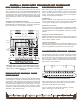
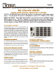
DX/256x256 SERIES MATRIX
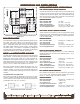
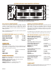
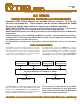
DX/256x256 Mainframe Rear View with IEEE488, RS232 and LAN Control
Shown with RS422 and RS232 Buffer Modules
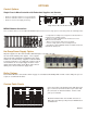
INPUT and OUTPUT BUFFERS
Optional Input and/or output buffer modules convert the system to
RS422 and/or RS232 levels. Each buffer module has sixty-four
(64) channels so a fully buffered 256x256 system has four input
buffers and four output buffers. When these modules are used, the
specifications of the system are determined by the input and/ or
output buffers present.
The RS422 input and output buffer modules have two options for
connectors, 68 pin male header or 78 pin female "D" connector.
RS422 Input Buffer Characteristic:
Common Mode Input Voltage (Vcm) -7V<Vcm<+7V
Differential Voltage Swing 200 mV Min
Input Resistance 6.8 KOhm Typical
Data Rate 20 Mb/s Max
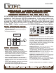
DX-256-2
The DX Series is intended to switch almost any digital stream data
stream in a non blocking (any input to any output without disturbing
previously set paths), full fan out (any one input to any or all out-
puts) configurations. The Basic system is intended to switch TTL or
CMOS signal levels.
When used without buffer modules, the system conforms to all TTL/
LVTTL specifications below
DX SPECIFICATIONS (signal w/o buffers)
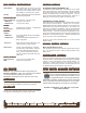
DX SPECIFICATIONS (signal with buffers)
Input Voltage High (VIH) : 2.1V Min 5.25V Max
Input Voltage Low (VIL) -0.3V Min 0.8V Max
Output Voltage High (VOH) 2.4V Min 3.7V Max
Output Voltage Low (VOL) --------- 0.4V Max
Data Rate --------- 80Mb/s Max
Output Current --------- 8 mA Max
CONNECTIONSCONNECTIONS
CONNECTIONSCONNECTIONS
CONNECTIONS
GENERAL SPECIFICAGENERAL SPECIFICA
GENERAL SPECIFICAGENERAL SPECIFICA
GENERAL SPECIFICA
TIONSTIONS
TIONSTIONS
TIONS
Signal Connections:
64 pin Headers or 78 pin female D connectors. Patch panels can
be provided to convert 64 pin headers or 78 pin female "D" to BNC,
SMA or customer specified connector.
AC Input: Universal, US Standard AC
RS232: D9 Male
GPIB: IEEE488
10BaseT LAN: RJ45
LAN to RS232: RJ45
RS422 Output Buffer Characteristic:
Common Mode Output Voltage 1.8V Typical
Output Voltage High (VOH) 2.5V Min /3.4V Max
Output Voltage Low (VOL) .3V Typical /.5V Max
Data Rate 20 Mb/s Max
Output Current 150 mA Max
RS-232 Input Buffer Characteristic:
Input Voltage Range -25V Min /+25V Max
Input Voltage High (VIH) 2.17V Min
Input Voltage Low (VIL) 1.06V Max
Data Rate 200 kb/s Typical
Input Resistance 5.0k Ohms Typical
RS-232 Output Buffer Characteristic :
Output Voltage High (VOH) +5V Min /+8V Max
Output voltage Low (VOL) -8V Typical /-5V Max
Data Rate 120 kb/s Typical
Output Current ±10mA Typical
Dimensions - 19" rack mount, 7" (4U) high and 20" deep
Weight - <45 lbs (20.41 Kg)
AC Input - 100 to 130 VAC or 200 to 260 VAC, 47/63 Hz,
Operating Temperature - 0 to 50 ºC
Storage Temperatures - -25 to 65 ºC
Switching Speed - 50 ns + Control Interface Delay
Humidity - 95% RH non condensing to 30º C
WARRANTY
CYTEC Corp. warrants that all products are free from defects in
Material or Workmanship for a period of five years
I
O
TTL to RS422
RS422 to TTL
TTL to RS232
RS232 to TTL
(D-78 Conns)
(D-78 Conns)
(3M Conns-68 pin)
A/C-IN
IEEE-488
RS-232
RS-232
UTP
L
I
N
K
OUTPUTINPUT
0-63
64-127
128-191
192-255
0-63
64-127
128-191
192-255
Output
Output
Output
Output
Input
Input
Input
Input