
Specifications

SPECIFICATIONS AND BUFFER OPTIONS
WARRANTY
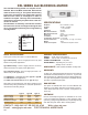
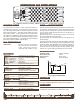
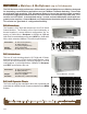
Connections BNC Signal Connections, AC input
and Remote Control input are on rear
panel shown in Fig.2. Alternate signal
connectors including SMA, SMB and
SMC optionally available.
ENVIRONMENTAL
POWER
AC Input Selectable 100-130 or 200-240
Volts AC, 50-60 Hz.
DC Supply Type Low Noise Linear
Consumption 150 Watts Maximum for 32x32 Matrix
VDX SERIES MATRIX
Operating Temperature 0
o
to 70
o
C
Storage Temperature -25
o
to 80
o
C
Humidity 95% RH noncondensing to 30
o
C
BANDPASS
CROSSTALK / ISOLATION
Small Signal 200 MHz (-3dB) for 200 mVpp
Flatness 0.1dB at 60 MHz
Large Signal 80 MHz (-2dB) for 2.0 Vpp
Flatness 0.1dB at 45 MHz
Slew Rate 0.375 V/ns
Crosstalk -50 dB at 5 MHz
-60 dB at 10 MHz Non Adjacent
-46 dB at 10 MHz Adjacent Channels
Isolation -95 dB at 10 MHz
MISCELLANEOUS
Switching Speed 50 ns plus any computer delay
Characteristic 75 Ohms (unbuffered)
Impedance 50 Ohms buffered
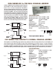
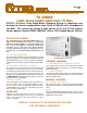
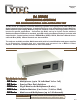
VDX/32x32 Mainframe with RS232 and LAN Control and BNC Signal Connections
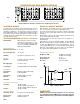
INPUT and OUTPUT BUFFERS
Optional Buffers are available for all Input and/or Output Chan-
nels. These buffers serve up to three different purposes:
1) They transform impedances to allow the solid state switch fab-
ric to be used for systems with other than 75 ohms characteristic
impedance.
2) Input Buffers can be used to reduce signals to levels where they
can be safely switched by the matrix.
3) Output Buffers can have preset gains to boost signals to re-
quired voltages.
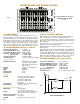
Rout
Rf
Rg
Ri
IN
Rs
OUT
A typical buffer is shown schematically in Fig. 3. Resistors Rs and
Ri set the input impedance and also attenuate the input signal (if
needed), while Rout determines the output impedance. The cir-
cuit is typically built with one of several standard small signal Op
Amps, but custom amplifiers are also possible. The specifications
for a typical small signal amplifier are shown below.
BUFFER SPECIFICATIONS
Bandpass (-3dB) 175 MHz w/ Vout=2Vpp
165 MHz w/ Vout=5Vpp
Preset Gains (Av) 2 to 16
Output Current 70 mA typical
Rise Time 0.375 V/ns typical
Input or Output Buffer
Fig. 2
Fig. 3
VDX-2
CYTEC Corp. warrants that all products are free from de-
fects in Workmanship and Materials for a period of five years
and that all switches are guaranteed for their Rated Opera-
tions.
The VDX Series is intended to switch small signal levels in a non-
blocking (any input to any output), full fan out (any input to any or
all outputs) configurations. The heart of the system is a solid state
32x32 switch fabric. When used without buffer amplifier modules,
the system conforms to all of the specifications shown below. When
used with input and/or output buffers, the specifications are deter-
mined by the buffer stages.
VDX SPECIFICATIONS (75 ohms, no buffers)
RS-232
UTP
LINK
RS-232