
User`s guide


DWMBB Adapter
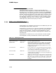
3.14.2.2 Transaction Register File in Loopback Mode Using DMA Writes and
Reads
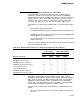
Figure 3–17 shows a way diagnostic software can use the diagnostic bits
and DMA loopback write/read pairs to test the DMA transmit and receive
registers as well as most of the control and data path of the DWMBB.
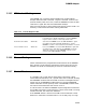
Figure 3–17 Testing the DMA Transmit and Receive Registers
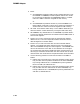
1. Do an I/O write to ADG1 to put DWMBB in DWMBB/A loopback mode:
2. Do a DMA loopback write/read pair with I/O Address Bit<2> set to zero:
3. Do a DMA loopback write/read pair with I/O Address Bit<2> set to one:
4. Do an I/O write to ADG1 to set DWMBB/A Flip FADDR<1> and Force Octaword Transfers:
I/O write − I/O data = 0000 0180#16
− I/O data
* The X’s in the address represent the node ID of the DWMBB.
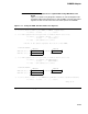
LOCATIONS TESTED:
TRANSMIT RECEIVE
DMAA C/A <41:0>
DMAA LW0 <31:0>
DMAA C/A <41:0>
DMAA LW1 <31:0>
0000 5555
msb−p098−89
I/O write − I/O address = XX XX00
= 5555
0000#16 *
5555#16
− same address as I/O write
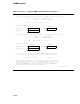
LOCATIONS TESTED:
00 5555
5555
I/O read
DMA LW0
AAAA AAAA#16
03C0#16
0000
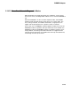
TRANSMIT RECEIVE
I/O write − I/O address = XX XXFF FFF7#16
=
0000
5555
00 AAAA AAAA
I/O read
DMA LW1
− I/O data
I/O write − I/O data =
− Same address as I/O write
00FF FFF7
AAAA AAAA
Figure 3–17 Cont’d on next page
3–143