
User`s guide


DWMBB Adapter
Table 3–19 (Cont.) Diagnostic Bits That Test DMA Buffers in Loopback Mode
Diagnostic Bit Location Description
Force DMA-A Buffer Busy
Force DMA-B Buffer Busy
ADG1<5>
ADG1<4>
When set, forces the DMA buffer control logic to place either the
DMA-A buffer or the DMA-B buffer into the busy state, forcing all DMA
traffic through the other buffer. Force DMA-A Buffer Busy and Force
DMA-B Buffer Busy ensure that both sets of DMA buffers get tested.
Setting both bits causes no DMA buffer to be available. The DWMBB
NO ACKs all VAXBI DMA transactions directed to it and NO ACKs any
further I/O transactions to it by "hanging." This verifies that a revision
J, or later, version of the DWMBB/B module contains a revision 5B,
or later, version BIIC since the DWMBB should hang after a DMA
loopback transaction with both DMA-A and DMA-B buffers busy.
The various settings follow:
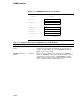
ADG1
<5:4> DMA Buffer Busy DMA Buffer Selected
0 0 None DMA-A
0 1 DMA-B DMA-A
1 0 DMA-A DMA-B
1 1 DMA-A and DMA-B None
DWMBB/B Flip Address
Bit<29>
BDCR1<4> Places the DWMBB in DMA loopback mode and converts I/O
transactions into DMA loopback transactions pointing to XMI memory
space.
DWMBB/B Flip Failing
Address Bit<1>
BDCR1<6> Used with Address Bit<2> of an I/O command to enable diagnostic
software to test all transmit and receive registers in the DWMBB/A
module gate array transaction register file. DWMBB/B Flip Failing
Address Bit<1> permits use of data buffers that would normally be
used only for transfers greater than a quadword.
This bit only affects DWMBB/B Failing Address Bit<1> when the
DWMBB/B module accesses data buffers in the transmit registers;
it does not affect the receive registers. DMA read data is stored in
the receive registers in the order it comes off the XMI. The bit has
no effect when accessing the C/A buffers in the transmit registers. It
controls which data buffers are used in loopback. Buffer access using
DWMBB/B Flip Failing Address Bit<1> and XMI I/O Address Bit<2> is
as follows:
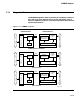
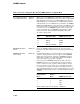
DWMBB/B Flip
Failing Address
Bit<1>
XMI I/O
Address
Bit<2> DMA Buffer Selected
00LW1
01LW2
10LW3
11LW4
NOTE: In DMA loopback mode, ADR<2> = FADDR<0>
3–140