
User`s guide


DWMBB Adapter
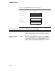
Table 3–19 (Cont.) Diagnostic Bits That Test DMA Buffers in Loopback Mode
Diagnostic Bit Location Description
DWMBB/A Flip Failing
Address Bit<1>
ADG1<9> DWMBB/A Flip Failing Address Bit<1> is used with Force Octaword
Transfer and XMI I/O Command/Address Bit<2> to allow diagnostics
to access and test all the transmit register files and receive register
files. DWMBB/A Flip Failing Address Bit<1> permits the use of the
data buffers that are used for transfers greater than a quadword. This
bit only affects DWMBB/A Failing Address Bit<1> when accesses
are made to data buffers in the transmit registers and not the receive
registers. DMA read data is stored in the receive register in the order
it comes off the XMI. This bit also has no effect when accessing the
C/A buffers in the transmit registers, but only controls which data
buffers are used in loopback mode. Buffer access using DWMBB/A
Flip Failing Address Bit<1> and XMI I/O Address Bit<2> is as follows:
DWMBB/A Flip Failing
Address Bit<1>
XMI I/O
Address<2> DMA Buffer Selected
00LW1
01LW2
10LW3
11LW4
NOTE: In DWMBB/A module loopback mode, XMI I/O Address<2> =
FADDR<0>.
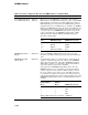
Force Octaword Transfers ADG1<6> When set, forces the length field of DMA transactions to have an
octaword status, allowing the testing of the upper two longwords of the
DMA buffers. When this bit is set, the four DMA buffer locations are
sent to the XMI, forming an octaword write, but only the one longword
selected by the setting of DWMBB/A Flip FADDR Bit<1> and XMI I/O
Address Bit<2> gets written. The mask of the octaword command
is zero for the other three longwords. Setting this bit during normal
operations causes undefined results.
3–139