
User`s guide


DWMBB/A Module Registers
Diagnostic 1 Register (ADG1)
bit<11>
Name: Force ECC Error
Mnemonic: None
Type: R/W, 0
Force ECC Error, when set, forces an ECC error to occur on any
transaction that reads the contents of a PMR. The error could be
either correctable or uncorrectable, depending on the data and check
bits stored in the selected PMR location.
bit<10>
Name: Force Transmit Lockout
Mnemonic: FORCE TLOCKOUT
Type: R/W, 0
Force Transmit Lockout, when set, forces the DWMBB/A module
to assert XMI TRANSMIT LOCKOUT L on the XMI, which is then
looped back into the DWMBB/A module as XMI RECEIVE LOCKOUT
L to test, with diagnostic software, the DWMBB/A module’s response
to XMI LOCKOUT L.
bit<9>
Name: DWMBB/A Flip Failing Address Bit<1>
Mnemonic: DWMBB/A FLIP FADDR BIT<1>
Type: R/W, 0
DWMBB/A Flip Failing Address Bit<1>, used together with I/O
Command/Address Bit <2> and Force Octaword Transfers (ADG1
<6>), enables diagnostic software to test all transmit and receive
registers in the DWMBB/A module gate array transaction register file.
This bit only affects accesses made to data buffers in the transmit
registers and not the receive registers. DMA read data is stored in the
receive register in the order it comes off the XMI. This bit also has no
effect when accessing the C/A buffers in the transmit registers, but
only controls which data buffers are used in loopback mode.
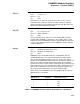
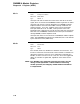
Buffer access using DWMBB/A Flip Failing Address Bit<1> and I/O
Address Bit<2> is as follows:
DWMBB/A Flip Failing
Address Bit<1> ADR Bit<2> DMA Buffer Selected
00LW1
01LW2
10LW3
11LW4
NOTE: In DWMBB/A module loopback mode, ADR<2> = FADDR<0>.
3–77