
Specifications

Accessing Device Interface Registers
2.6 Constructing a Mailbox Command Within a CRAM
2.6.1 Register Data Byte Lane Alignment
The CRAM routines supplied by OpenVMS AXP enforce a longword oriented
view of I/O adapter register space, which means that adapter register space is
viewed as if register bytes occupy a 32 bit data path, as follows:
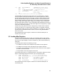
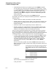
Adapter Register space
31 24 23 16 15 8 7 0 offset
byte 3 byte 2 byte 1 byte 0 0
byte 7 byte 6 byte 5 byte 4 4
etc
Write example: To write a byte to register byte 2, specify IOC$CRAM_CMD
parameters as follows:
command_index = cramcmd$k_wtbyte32
byte_offset = 2
adp_address = adp address
cram_address = cram address
The data to be written must be positioned in bits 23:16 of the write data field
(CRAM$Q_WDATA).
Read example: To read a byte from register byte 2, specify IOC$CRAM_CMD
parameters as above except use CRAMCMD$K_RDBYTE32 as the command_
index.
The data from register byte 2 will be returned in bits 23:16 of the CRAM read
data field (CRAM$Q_RDATA).
The programmer must perform the proper byte lane alignment of data for register
writes. On register reads, the data is returned in its natural byte lane without
any shifting. Note that this way of looking at adapter register space maps
directly to the semantics of most I/O buses, but is distinctly diferent from VAX
behavior.
2.7 Initiating a Mailbox Transaction
An OpenVMS AXP device driver initiates to a device register by issuing a calls to
IOC$CRAM_IO.
2–7