
Specifications


5/9/13 888-2857-001 4-11
WARNING: Disconnect primary power prior to servicing.
Section 4 Theory of Operation
Platinum VAX-C Series
4.4.6 ASI / SMPTE 310 Inputs / Output
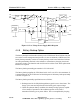
The modulator FPGA decodes the four ASI inputs and modulates the active input
stream with the selected standard. Transformers are used on the input of the ASI data to
improve the rejection of common mode interference on the input cables. Cable
equalization circuitry is also used. The ASI inputs to the FPGA are at LVDS levels.
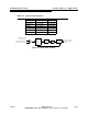
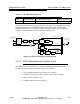
Input choices are shown below, rear panel connectors
are shown to the right.
• 1 -> ASI input (HP 1) for DVB modulation stan-
dard (top left connector)
• LP 1 -> ASI Input, LP 1 for DVB input, ATSC this
will be the second ASI input, all other standards
this is not used. (top right connector)
• 2 -> Secondary ASI input for all OFDM modulation standards. Also known as HP 2
for DVB. Primary SMPTE input for ATSC (bottom left connector)
• LP 2 -> ASI Input, LP 2 for DVB input, ATSC this will be the second SMPTE input,
all other standards this is not used. (bottom right connector)
NOTE:
LP1 and LP2 inputs are used only for COFDM Hierarchial modes.
The modulator FPGA also provides an ASI monitor output. The ASI monitor output is
at LVDS levels from the FPGA. It utilizes an LVDS (Low Voltage Differential Signal)
driver and transformer per the ASI specification.
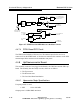
The DUC (Digital Up Converter) FPGA is responsible for taking the modulated data
and applying correction, as well as up converting the baseband signal allowing the
system to come out on the correct frequency to feed to the DAC. The DUC FPGA
output data is then transferred to the DAC to be converted to a 140 MHz IF, which is
then up-converted to the on channel frequency.
The DUC writes the 16-bit I and Q data to the AD9779 DAC. The DAC will be clocked
by the ~409 to 460 MHz clock from the PFRU. The 1/4 F
DAC
clock output of the DAC
is used as a clock for the DUC FPGA and the RF Sample ADC. The DAC provides the
Up/Downconverter board with the 140MHz IF.
The AD9461 ADC is clocked by the 1/4 FDAC clock. It converts the 140 MHz IF from
the downconverter to a 16 bit sample provided to the DUC FPGA. The ADC also
provides the DUC FPGA with the sample A/D clock.