
Instruction manual


Once the console has ascertained the size of each bank, it writes the correct
values into the MCRs.
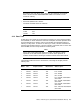
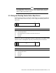
The next table describes a set of sample MCRs, representing a system containing
five banks located in random slots with memory sizes:
128 MB
128 MB
32 MB
32 MB
8MB
MCR#
Bank
Size Compare<29:23> Mask<26:23> Address Space
0 0 MB 111xxxx xxxx
1 0 MB 111xxxx xxxx
2 32 MB 01000xx 0011 256 - 287 MB
3 32 MB 01001xx 0011 288 - 319 MB
4 8 MB 0101000 0000 320 - 327 MB
5 0 MB 111xxxx xxxx
6 128 MB 000xxxx 1111 000 - 127 MB
7 128 MB 001xxxx 1111 128 - 255 MB
In this case, the console must pass a maximum memory size of 328 MB to the
operating system, so that it never reference banks 0, 1, and 5.
4.1.3 Improper Configuration
If the CPU performs a read operation on a nonexistent bank of memory,
UNPREDICTABLE data are returned.
If the CPU issues a read to a bank of memory whose actual size is smaller than
the MCR register indicates, then the address wraps around in that bank.
4.1.4 Disabling Memory
Memory can be disabled bank-by-bank. If the compare and mask bits indicate
that a bank occupies an area of memory higher than the size recorded by the
operating system, it never accesses that bank.
In the previous table of MCRs, banks 0, 1, and 5 are never accessed because their
address space (<29:27> = <111>) is higher than the largest address (328 MB) that
the operating system will accesses.
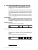
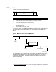
The address for a write operation to an MCR is:
07 06 05 04 03 02 01 0011 10 09 0815 14 13 1221 20 19 1829 17 1628 27 26 25 24 23 2231 3033 32
0 1 C22 Compare<29:23> Mask<26:23> X XXX
MR−0169−93RAGS
XMCR#0
4–4 Address ASIC Registers (400/500/600/700/800/900 Models)