
Instruction manual
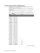

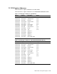

7.3.18 SCC-0 DMA Slot Register—1.A004.0180/1.E004.0180
This and other DMA slot registers were included in the hardware for future
implementations of the address decoding.
The register’s format and contents are:
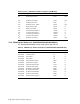
Bits Access Reset Function
3:0 R/W UNP Chip selects. Must be set to 4; otherwise, registers
cannot be written to.
9:4 R/W UNP Hardware address supplied for SCC-0 DMA
accesses. Must be set to 1. Control hardware
decoding of addresses supplied for SCC-0 DMA
accesses.
31:10 0 Reserved, returns 0 when read
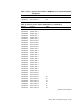
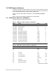
7.3.19 SCC-1 DMA Slot Register—1.A004.0190/1.E004.0190
This and other DMA slot registers were included in the hardware for future
implementations of the address decoding.
The register’s format and contents are:
Bits Access Reset Function
3:0 R/W UNP Chip selects. Must be set to 6; otherwise, they
cannot be written to. Control hardware decoding of
chip selects for SCC-1.
9:4 R/W UNP Hardware Address supplied for SCC-1 DMA
accesses. Must be set to 1. Control hardware
decoding of addresses for DMA on SCC-1.
31:10 0 Reserved; returns 0 when read
IOCTL ASIC and System Registers 7–17