
User's Manual

VT-MOD-CELL-B48 Hardware User Manual
3
2. Interface
2.1 Overview
This chapter mainly introduces the external interfaces of VT-MOD-CELL-B48 LTE
module, including:
LCC Interface
Antenna Interface
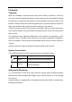
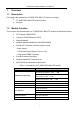
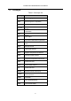
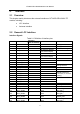
2.2 General LCC Interface
Interface Signals
Table 2-1 Definition of interface pins
Pin No.
Pin Name
Direction
(Refer to module)
Pin Definition Remarks
1 Reserved
floating
2 Reserved
floating
3 SPI_CS2# O SPI chip selection If not use, floating
4 SPI_MISO I
SPI data bus (Master
input, Slave Output)
5 SPI_SCLK O
6 SPI_MOSI O
SPI data bus (Master
input, Slave Output)
7 GND
8 UART1_TXD O UART1 data transmit
9 UART1_RXD I UART1 data receive
10 UART0_TXD O UART0 data transmit
Debug interface
11 UART0_RXD I UART0 data receive
12 WPS_KEY
WPS button
13 GND
14 SDH0_D3
SDIO0 data 3
SDIO0 interface for
2.5G Wi-Fi; if not used,
floating;
15 SDH0_D2
SDIO0 data 2
16 SDH0_D1
SDIO0 data 1
17 SDH0_D0
SDIO0 data 0
18 SDH0_CMD
SDIO0 data command
19 SDH0_CLK
SDIO0 clock
20 GND
21 Reserved
Floating
22 WI-FI_RST#
O
Wi-Fi reset
Wi-Fi reset
23 GPIO_GPD4
O
GPIO
LTE RF Signal
Strength 3
24 GPIO_GPD2
O
GPIO
LTE RF Signal
Strength 1
25 GPIO_GPD6
O
GPIO
2.4G Wi-Fi_LED
&WPS_LED
26 GPIO_GPD3
O
GPIO
LTE RF Signal
Strength 2