
Specification Sheet

6
www.v-color.com.tw
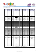
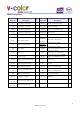
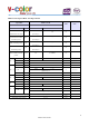
Absolute Maximum Ratings
Symbol
Parameter
Rating
Units
Notes
VDD
Voltage on VDD pin relative to Vss
- 0.4 V ~ 1.80 V
V
1,3
VDDQ
Voltage on VDDQ pin relative to Vss
- 0.4 V ~ 1.80 V
V
1,3
VIN, VOUT
Voltage on any pin relative to Vss
- 0.4 V ~ 1.80 V
V
1
TSTG
Storage Temperature
-55 to +100
°C
1, 2
Notes:
1. Stresses greater than those listed under “Absolute Maximum Ratings” may cause permanent damage to
the device. This is a stress rating only and functional operation of the device at these or any other conditions
above those indicated in the operational sections of this specification is not implied. Exposure to absolute
maximum rat ing conditions for extended periods may affect reliability.
2. Storage Temperature is the case surface temperature on the center/top side of the DRAM. For the measurement
conditions, please refer to JESD51-2 standard.
3. VDD and VDDQ must be within 300mV of each other at all times; and VREF must not be greater than
0.6XVDDQ,When VDD and VDDQ are less than 500mV; VREF may be equal to or less than 300mV.
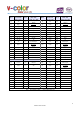
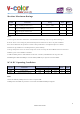
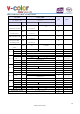
AC & DC Operating Conditions
NOTE:
1.Under all conditions, VDDQ must be less than or equal to VDD.
2.VDDQ tracks with VDD. AC parameters are measured with VDD and VDDQ tied together.
Symbol
Parameter
Rating
Unit
NOTE
Min.
Typ.
Max.
VDD
Supply Voltage
1.425
1.500
1.575
V
1,2
VDDQ
Supply Voltage for Output
1.425
1.500
1.575
V
1,2