
User Manual

RPC Installation RPC/RP Manual
WLL-RPC/RP-IN/UM-1.0 19June2000
2-
8
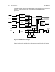
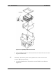
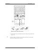
internally with the E1IF through the backplane busses and the switch in the ECNT
module. Refer to Figure 2-7 for a block diagram of the RPIF module’s
processing.
RPIF
RPIF
RPIF
RPIF
Layer 1
LSI
Layer 1
LSI
Layer 1
LSI
Layer 1
LSI
-116V
+5V
Time slot
Assignment
Controller
HDLC
Controller
CPU
(16 bit)
Bus
Controller
DPRAM
RAM
ROM
Address Bus
Data Bus
ADPCM Highway
ADPCM Highway
PCM
Clock/ Frame
signal
Generator
ADPCM Clock
Internal
BUS
Figure 2-7: RPIF Module Block Diagram
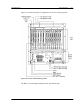
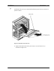
Figure 2-8 shows the module’s physical configuration and describes the function
of the LEDs and the reset switch.