
Technical information

K630 - V640 - K660
1215-3608 rev. 1
APPENDIX
APPENDIX
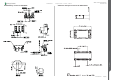
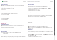
PIN CONNECTIONS
A3
B3
C3
A2
B2
C2
A1
B1
C1
INM OUTA INP
VM_P VM V
p
BYPASS OUTB SHUTDOWN
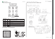
9−Pin Flip−Chip CSP
(Top View)
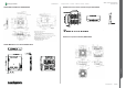
Pin conguration (Bump side)
12345
A
B
C
D
VMIC SPRi
SPLi
MIC
Ni
MIC
Pi
INT
mice
Gnd
INT
mici
CCO VAD
Gnd
Gnd
Gnd
Gnd
Gnd
SPR
e
SPL
e
MIC
Ne
MIC
Pe
SPR
EF
1234152345
A
B
C
D
A
B
C
D
VMIC SPRi
SPLi
MIC
Ni
MIC
Pi
INT
mice
Gnd
INT
mici
CCO VAD
Gnd
Gnd
Gnd
Gnd
Gnd
SPR
e
SPL
e
MIC
Ne
MIC
Pe
SPR
EF
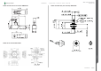
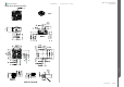
Electrical diagram
SPRi
SPLi
MICPe
GND
SPRe
SPREF
MICPi
MICNi
CCO/VMICVAD
MICNe
INTmici
SPLe
GND
CCO/VMIC
INTmice
R1
R7
R8R6
R4
R5
R3
R2
SPRi
SPLi
MICPe
GND
SPRe
SPREF
MICPi
MICNi
CCO/VMICVAD
MICNe
INTmici
SPLe
GND
CCO/VMIC
INTmice
R1
R7
R8R6
R4
R5
R3
R2
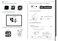
PIN DESCRIPTION
Pin Type Symbol Description
A1 I INM Negative input of the first amplifier, receives the audio input signal. Connected to the
feedback resistor R
f
and to the input resistor R
in
.
A2 O OUTA Negative output of the NCP2892. Connected to the load and to the feedback resistor Rf.
A3 I INP Positive input of the first amplifier, receives the common mode voltage.
B1 I VM_P Power Analog Ground.
B2 I VM Core Analog Ground.
B3 I V
p
Positive analog supply of the cell. Range: 2.2 V−5.5 V.
C1 I BYPASS Bypass capacitor pin which provides the common mode voltage (Vp/2).
C2 O OUTB Positive output of the NCP2892. Connected to the load.
C3 I SHUTDOWN The device enters in shutdown mode when a low level is applied on this pin.
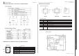
Components - N3100, N3101, S2400-03
N3100 IC Amp RYT109914/1
N3101 EMI Filter and ESD ROP1013074/1
S2400-03 Input Side Switch Push RMD 10116/9
SEMC Troubleshooting Manual
82 (96)