
Technical information

K630 - V640 - K660
1215-3608 rev. 1
APPENDIX
APPENDIX
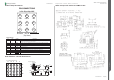
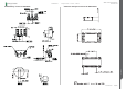
(TOP VIEW)
C3 C1
IN OUT
B2
GND
A3 A1
NR EN
PIN DESCRIPTIONS
TPS799xx
DESCRIPTION
NAME YZU
IN C3 Input supply.
GND B2 Ground
Driving the enable pin (EN) high turns on the regulator. Driving this pin low puts the regulator into
EN A1
shutdown mode. EN can be connected to IN if not used.
Fixed voltage versions only; connecting an external capacitor to this pin bypasses noise generated
NR A3
by the internal bandgap. This allows output noise to be reduced to very low levels.
Adjustable version only; this is the input to the control loop error amplifier, and is used to set the
FB A3
output voltage of the device.
Output of the regulator. A small capacitor (total typical capacitance ≥ 2.0μF ceramic) is needed from
OUT C1
this pin to ground to assure stability.
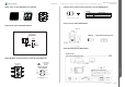
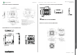
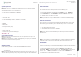
Connection Diagrams
Pin Descriptions
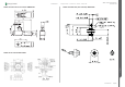
noitpircseDemaN#niP
A1 PV
IN
Power Supply Voltage Input to the internal PFET switch.
B1 V
DD
Analog Supply Input.
C1 EN Enable Input. Set this digital input high for normal operation. For shutdown, set this pin low.
C2 V
CON
Voltage Control Analog input. V
CON
controls V
OUT
in PWM mode.
C3 FB Feedback Analog Input. Connect to the output at the output lter capacitor.
B3 SGND Analog and Control Ground
A3 PGND Power Ground
A2 SW Switch node connection to the internal PFET switch and NFET synchronous rectier.
Connect to an inductor with a saturation current rating that exceeds the maximum Switch Peak
Current Limit specication of the LM3208.
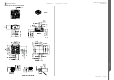
Block Diagram
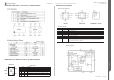
Components - N2203, N2204, N2205
N2203 2CH-LDO Vout1 = 2.8V Vout2 = 1.8V RYT113997/4
N2204 LDO 1.2V, 200mA Low Noice CS 5 RYT1137816/3
N2205 IC Vreg 1200-0107
SEMC Troubleshooting Manual
81 (96)