SEMC Troubleshooting Manual K630 - V640 - K660 ABOUT Troubleshooting Manual TROUBLESHOOTING MEASUREMENT POINTS COMPONENT OVERVIEW FUNCTIONAL OVERVIEW K630 - V640 - K660 APPENDIX 1215-3608 rev.
ABOUT SEMC Troubleshooting Manual K630 - V640 - K660 Contents ABOUT The purpose of this document is to provide enhanced technical information for Sony Ericsson repair technicians in order to assist during service, repair and troubleshooting operations on Sony Ericsson mobile phones. It should be used as a complement to other repair instructions and tools as notified by the local Sony Ericsson representative.
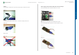
TROUBLESHOOTING Equipment List SEMC Troubleshooting Manual K630 - V640 - K660 K630, V640 and K660 Equipment List TRS Fixture Kit K630 and V640 K630 and V640 Location: CSPN-Repair Instructions-Electrical- K630, V640 -Equipment List TROUBLESHOOTING K660 Location: CSPN-Repair Instructions-Electrical-K660 -Equipment List Dummy Battery K630 and V640 Location: CSPN-Repair Instructions-Electrical- K630, V640 -Equipment List Part number: NTZ 112 533 K660 Location: CSPN-Repair Instructions-Electrical-K660 -E
TROUBLESHOOTING Location: CSPN-Repair Instructions-Level: Mechanical-Tool Catalogue The 0, 64 mm Test Probes is recommended by Sony Ericsson when DMM is in use see picture 1.
TROUBLESHOOTING Cables USB Computer Cable Location: CSPN-Repair Instructions-Level: Mechanical-Tool Catalogue See Picture 4.
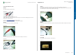
TROUBLESHOOTING STEP 3: Cut off isolation material from inside of the charger plug according to Picture 9. Equipment List SEMC Troubleshooting Manual K630 - V640 - K660 Power Supply Channel 2 DCIO/SEPI Cable Connection Setups Correct DCIO/SEPI Cable setup when TRS Fixture is used. Picture 9 Picture 12 TROUBLESHOOTING STEP 4: Connect DCIO and SEPI Interface Cable – A1 cables according to Picture 10. Picture 10 Note: Example of DCIO/SEPI and K750 TRS Fixture Setup.
TROUBLESHOOTING Equipment Equip ment List SEMC Troubleshooting Manual K630 - V640 - K660 Picture 15 Picture 18 TROUBLESHOOTING STEP 1: Use Cable according to Picture 15 STEP 4: Use only wire connected to Pin2 and cut all other wires according to Picture 18. Use a digital multimeter instrument (DMM) and perform diode measurement to select the wire connected to Pin2 at hands free system connector plug.
TROUBLESHOOTING Equipment List Test SIM GSM/UMTS One Test SIM GSM/UMTS is needed to perform Current Consumption Test, see Picture 21. Location: To buy a Test SIM GSM/UMTS, please contact your supplier of test equipment.
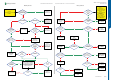
TROUBLESHOOTING SEMC Troubleshooting Manual K630 - V640 - K660 On/Off Problems - Flash Problems On/Off problems START Flash problems Is the phone consuming more than 1mA when the phone is powered off Connect: Dummy Battery connected to VBATT Go to Dead phone Problems part 1 Yes Yes Is it possible to power on the phone Yes Is it possible to power off the phone Yes Go to Current Consumption Test After this go to Charging Test.
TROUBLESHOOTING START SEMC Troubleshooting Manual K630 - V640 - K660 Dead Phone problems part 2 Dead Phone problems part 1 Step 1: Try to recover the phone using EMMA III SW Press keys 2 and 5 Connect USB Cable Run pre-config 1 or 2 Run DPY/Z S2400 Not pressed Using more than 1mA current No K660: Replace B2100 K630/V640: SL 5 Replace B2100 SL 4 Escalate Keep S2400 Pressed or Connect DCIO/SEPI Cable Dead Phone problems Part 2 (Dead Phone Problems Part 1 must be finished before starting here) VBT27
TROUBLESHOOTING SEMC Troubleshooting Manual K630 - V640 - K660 Display Problems - Display Illumination Problems Display Illumination problems Display problems START No Display Backlights Ok Yes Step 1: Use TRS Fixture and connect Display and Keypad.
TROUBLESHOOTING Key problems LED problems START SL 5 Replace V2402 SL 4 Escalate DMM Settings: Problem with Phone On No Yes Yes 0 Volt DC between MP 83 (S2402 A) and MP 82 (S2402 C) No Short Circuit between MP 83 (S2402 A) MP 92 (PBA GND) and MP 82 (S2402 C) MP 92 (PBA GND) Problem with Volume Up key Yes Remove S2402 More than 2.
TROUBLESHOOTING Main and VGA Camera problems Vibrator problems START Are there problems with both Main and VGA Camera Claim VGA Camera START Go to Service Tests and Perform: Main and VGA Camera Test Yes VGA Camera Ok No No Load ITP SW into the phone. Use TRS Fixture and connect Display. Main and VGA Camera mounted on the PBA.
TROUBLESHOOTING Charging problems Use TRS Fixture and Fault Trace SW Connect: VBATT and DCIO/SEPI Start Battery Calibration Current Calibration Passed Yes Yes START 5 Volt DC at MP 25 (ST2201) Is MP 87 (TP2202) Short circuit to PBA GND Yes Step 1: Perform System Connector Protection Test If step 1 is Ok then continue with step 2.
TROUBLESHOOTING SIM Problems - Memory Stick Problems SEMC Troubleshooting Manual K630 - V640 - K660 Memory Stick problems SIM problems START Flash the Phone with EMMA SUCR SW Sim Com Test Passed Yes Remove Test SIM Disconnect: Dummy Battery Use TRS Fixture and Fault Trace SW Load ITP SW into the phone.
TROUBLESHOOTING Audio Internal problems Yes 2.6 Volt DC At MP 121 (V2420) No Audio External problems Go to Audio External Problems SL 4 Replace V3101 or V3102 SL 5 Replace L3103 or L3104 SL 5 Replace R2440 SL 4 Escalate No START 2.
TROUBLESHOOTING FM Radio problems Replace N3101 PHF working properly during Voice call No SL 5 Replace N2000 SL 4 Escalate Bluetooth problems START Speaker and FM Radio Tests working properly Yes SEMC Troubleshooting Manual K630 - V640 - K660 FM Radio Problems - Bluetooth Problems Go to Service Tests and Perform: Speaker and FM Radio Test Flash the phone with the EMMA SUCR SW and retest the phone. If successful claim SW Flashing If not then continue with Bluetooth problems TRS guide.
TROUBLESHOOTING GSM Network problems 0 Ohm between MP 85 (R1208) and MP 81 (R1202) START No Is Max Pwr 23dBm Ok (±3dBm) Yes 2.8 Volt DC at MP 36 (R2202 VccA) SL 5 Replace N2000 SL 4 Escalate No Instrument Settings: System Mode: TX/RX Tester Mode (WCDMA) Downlink Channel: 10562 Measurement Mode: Repeat Correction: 1.
TROUBLESHOOTING System Connector Protection Test - Current Consumption Test SEMC Troubleshooting Manual K630 - V640 - K660 Current Consumption Test System Connector Protection Test Perform Diode and Ohm measurements with a Multimeter Connect the black probe at ground (Pin 9 on the system connector, X2400) Step 1: Insert Local SIM Card and use the phone with the Normal SW (SSW) and dummy battery connected to Power Supply Channel 1 VBATT according to Picture 1. Instrument settings: Voltage: 3.
TROUBLESHOOTING Step 4 with Fault Trace SW application: - Flash the phone with ITP SW Use the TRS Fixture Connect the: Power Supply Channel 2 DCIO/SEPI Instrument settings: Voltage: 5 Volt, Limiter 2A - Connect DCIO/SEPI Cable to the phone - Max TX Power WCDMA BAND I Fault Trace SW settings: TX and RX WCDMA Radio Settings: Select Band: BAND I Fast Select Channels: Ch LOW Modes: Max Pwr 23dBm Compare the current consumption during Max TX Power Tests with the current consumption limits below.
TROUBLESHOOTING SEMC Troubleshooting Manual K630 - V640 - K660 Battery and Current Calibration Test - Backup Capacitor Test Backup Capacitor Test Battery and Current Calibration Test To perform this test use: Use the Phone with the ITP SW - Phone with the ITP SW Power Supply Channel 1 VBATT: X Volt according to the Fault Trace SW Test Instructions: Fault Trace SW-Logic-Phone Power-Battery Calibration and follow test instructions. Limiter: 2A.
TROUBLESHOOTING - Phone with the Normal SW (SSW) Dummy Battery connected to Power Supply Channel 1 VBATT Power Supply Channel 1 VBATT instrument settings: Voltage: 3.0 to 4.2 Volts, according to VBATT row in the Reference Table. Limiter: 2A Power Supply Channel 2 DCIO/SEPI instrument settings: Voltage: 5V Limiter: 2A The purpose with this test is to check following items: - The following ASICs are tested: - Test instructions: - Reference Table VBATT x Volt Test Time x sec.
TROUBLESHOOTING Voltages to N2000 MP Pnone Off Phone On Phone Off Phone On Voltages from N2000 MP Phone Off Phone On Clocks to N2000 MP Phone Off Phone On Clocks from N2000 MP Phone Off Phone On VCORE18 from N2202 MP Phone Off Phone On MP 63 (X2200 Pin 3) VBAT 3.8V 3.8V MP 89 (TP2200) VBATI 3.8V 3.8V MP 87 (TP2202) BDATA 0.00V 0.00V MP 26 (C2242) VDD_REF 3.8V 3.8V MP 41 (ST2204) VAUDIO26 0.00V 0.00V 2.6V MP 34 (ST2203) VANA25 0.00V 0.00V 2.5V MP 33 (ST2208) VDDE18 0.00V 0.00V 1.
MEASUREMENT POINTS SEMC Troubleshooting Manual K630 - V640 - K660 Front Side MP 1 MP 2 MP 3 MP 4 MP 5 MP 6 MP 7 MP 8 MP 9 MP 10 MP 11 MP 12 MP 13 MP 14 MP 31 MP 32 MP 33 C4329 ST4317 C4222 Same net only 1 Same net only Same net only Same net only Same net only Same net only MP 35 R1205 D2105 C2303 MP 36 C2342 C4225 C2328 R2101 ST2106 C4224 C2304 C2327 C4226 R2100 C4223 R2120 R2118 2 Same net only Same net only Same net only Same net only Same net only C4227 D
TP3104 MP 54 MP 55 MP 56 MP 57 MP 58 MP 59 MP 60 TP2206 TP2207 MP 61 Mp 62 MP 63 MP 64 MP 65 MP 66 MP 67 MP 68 MP 69 MP 70 MP 71 MP 72 MP 73 MP 74 MP 75 TP2205 MP 76 MP 78 MP 77 C2 4 2 7 MP 53 C2461 MP 52 C2459 MP 51 C2462 MP 50 C2460 MP 49 C2464 MP 48 X3103 MP 47 X3102 MP 46 SEMC Troubleshooting Manual K630 - V640 - K660 Back Side C2463 MEASUREMENT POINTS MP 110 TP3105 TP2003 TP2203 C2448 C302 Z1000 C2457 C2456 C2458 C2470 C2469 C2467 C2465 C24
MEASUREMENT POINTS VBATI VDIG VDDE18 VCC_WPA VccA VAUDIO26 VBT27 VDIG VCAMSD28 VCAMSD28 VBEAR26 SEMC Troubleshooting Manual K630 - V640 - K660 Top Schematic VCAMSD13 VCAMSD18 VCAMSD18 VDDE18 VCAMSD13 VBATI VBATI VBOOST VDDE18 VDIG VccA VCC_WPA VBATI VBT27 VDDE18 VAUDIO26 KB_LED VBOOST VBEAR26 VDIG KB_LED2 VCAMSD13 VCAMSD28 VCAMSD28 VCAMSD18 VCAMSD18 KB_LED KB_LED I2CCLK1 I2CCLK1 I2CDAT1 I2CDAT1 BT_CLKREQ VAD BTRESn BTRESn Imaging VAUDIO26 VBATI MICP/AUXinL VBT27 VBEA
MEASUREMENT POINTS BT_CLKREQ BT_CLKREQ MCLK MCLK VDDE18_ANJA VAUDIO26 VMC18 VDDE18 VBATI VDDE18_ANJA VDDE18 VDD_LP VBATI VAD SPL SPR VAD TX_ADSTR SPL SPR VDDE18 VDDE18_ANJA CAMSYSCLK BT_CLKREQ MCLKREQ MCLK SERVICEn SERVICEn ONSWAn ONSWAn TESTOUT VAD I2CDAT1 TX_ADSTR I2CCLK1 SPL MICN/AUXinR SPR MICP/AUXinL VBOOST SERVICEn BTRESn ONSWAn FMRESn RTCCLK RTCCLK BT_CLK BT_CLK CAMSYSCLK CAMSYSCLK MCLKREQ MCLKREQ BTRESn BTRESn FMRESn FMRESn System Control I2CDAT1 I2CDAT
MEASUREMENT POINTS SEMC Troubleshooting Manual K630 - V640 - K660 System Top VDDE18 VDD_LP VDDE18 VDD_LP VDDE18 VDDE18 VDD_LP BT_CLK CAMSYSCLK RTCCLK MCLKREQ BT_CLKREQ MCLK SERVICEn ONSWAn BT_CLKREQ MCLK SERVICEn ONSWAn MEASUREMENT POINTS VDD_LP BT_CLK CAMSYSCLK RTCCLK MCLKREQ BT_CLK CAMSYSCLK RTCCLK MCLKREQ BT_CLKREQ MCLK BTRESn SERVICEn FMRESn ONSWAn BTRESn FMRESn BTRESn FMRESn MEMRESn Clocks & Resets MEMRESn MEMRESn VDDE18_ANJA VDDE18_ANJA VDDE18_ANJA Memories Made for Applic
MEASUREMENT POINTS SEMC Troubleshooting Manual K630 - V640 - K660 System Control - Clocks & Resets VDDE18 VDD_LP RTCCLK VDDE18 VDDE18 RTCCLK VDDE18 VDD_LP R2121 10ohms R2119 100Kohms R2120 0ohms D2105 1 OE 2 A 5 Y VCC GND R2118 68ohms 4 3 R2101 100Kohms BT_CLK BT_CLK MP 10 SN74LVC1G125YZPR 1200-0425 1A C2121 4.
MEASUREMENT POINTS SEMC Troubleshooting Manual K630 - V640 - K660 System Memories D2000 Anja-PoP bottom - SYSTEMLEVEL APPLICATION MEMORYIF(EMIF2) D2000 Anja-PoP bottom - SYSTEMLEVEL E4 F4 F5 AP_D00 AP_A01 D12 AP_D01 AP_A02 B15 B12 AP_D02 AP_A03 C15 E16 AP_D03 AP_A04 B16 C16 D14 AP_D04 AP_A05 SH_A01 D2 D15 AP_D05 AP_A06 C17 SH_D01 SH_A02 E2 D16 AP_D06 AP_A07 C18 SH_D02 SH_A03 J10 E15 AP_D07 AP_A08 SH_D03 SH_A04 F2 E17 AP_D08 AP_A09 B19 E18 SHARED MEMORY IF (EM
MEASUREMENT POINTS SEMC Troubleshooting Manual K630 - V640 - K660 PoP IF TOP_SH_DATA_BUS D2020 D2000 TOP_APPLICATION_DATA_BUS 1GbitNANDx8+512MbitSDRAMx16 Anja-PoP_top-SYSTEM-LEVEL SHAREDMEMORYIF(EMIF1) SHARED_MEMORY-IF(EMIF1) D2020 D2000 TOP_SH_A01 T20 SDRAM_A0 SDRAM_DQ0 B7 TOP_SH_D00 Anja-PoP_top-SYSTEM-LEVEL 1GbitNANDx8+512MbitSDRAMx16 T_A6 SH_D01 SH_A02 T_U21 TOP_SH_A02 U21 SDRAM_A1 SDRAM_DQ1 A6 TOP_SH_D01 APPLICATION_MEMORY-IF(EMIF2) APPLICATIONMEMORYIF(EMIF2) TOP_SH_D02 T_B
MEASUREMENT POINTS SEMC Troubleshooting Manual K630 - V640 - K660 Power Top VBATI VBATI VCAMSD13 VCAMSD28 VCAMSD18 CAM_LDO_EN VCAMSD13 VCAMSD28 VCAMSD18 CAM_LDO_EN VCAMSD13 VCAMSD28 VCAMSD18 CAD_LDO_EN Power Camera MEASUREMENT POINTS VCORE18 Power Memories VDDE18 VANA25 VCORE12 VDDE18 VANA25 VDDE18_ANJA VDDE18_ANJA VDDE18_ANJA VCORE12 Power Asics VBUS DCIO VBUS DCIO VBUS VBATI DCIO VCORE18 VDDE18 VANA25 VCORE12 VMC18 VAUDIO26 VBT27 VDIG VBEAR26 VBACKUP VccA VCC_WPA WPAVCC DCDC_EN WP
SEMC Troubleshooting Manual K630 - V640 - K660 Power Regulators & Charging VDD_LP VDDE18 VDD_LP N2000 Ericsson AB 3100 POWER TP2200 K14 MP 87 1000-0412 C2211 22pF TP2202 TP2201 F14 C2212 3.3pF LDOG 1.5 - 2.85V LDOD 2.65V VBAT_B 3 1 Strap ST2203 2 1 Strap ST2208 2 1 Strap ST2212 2 1 Strap ST2213 2 1 Strap M13 VBAT_F LDOH 1.2 - 2.75V LDOK 1.8 - 2.75V R2200 25mohms V2200 2 A GND N14 0.1uF C2206 1 C 1 VBAT_G VANA25 VDDE18 VBT27 VDIG VDIG VBEAR26 MP 31 C2225 2.
MEASUREMENT POINTS SEMC Troubleshooting Manual K630 - V640 - K660 Power Camera VBATI VCAMSD28 VCAMSD18 VCAMSD13 VBATI VCAMSD13 VCAMSD18 VCAMSD28 MEASUREMENT POINTS CAM_LDO_EN VBATI CAM_LDO_EN MP 61 MP 47 N2204 D2000 APPLICATION GPIO_04 VCAMSD13 TP2205 LDO REGULATOR R25 ANJA-Bottom 1200-0186 R2280 100Kohms A1 EN C3 IN B2 GND ST2281 TPS79913YZU 1200-1852 OUT C1 NR A3 2 1 Strap 1.3 C2287 C2286 1uF C2288 4.7uF 0.
MEASUREMENT POINTS SEMC Troubleshooting Manual K630 - V640 - K660 Power ASICs D2000 Anja-PoP bottom - POWER GND (logic & I/O) VANA25 VCORE12 GND D2000 GND J22 VDD I/O (analog) GND K16 AB8 VDDIO_2V5 GND K17 AB15 VDDIO_2V5 GND K18 D2000 VDD ANALOG Anja-PoP bottom - POWER VDDCORE (logic) VDDCO_1v2 B6 VDDCO_1v2 B9 VDDCO_1v2 B17 VDDCO_1v2 B24 VDDCO_1v2 AD3 VDDCO_1v2 AD24 VDDCO_1v2 AD25 VDDCO_1v2 AE2 VDDCO_1v2 AE24 VDDCO_1v2 AC14 GND L14 VSSAD AE11 GND L15 AB13 VD
MEASUREMENT POINTS VCORE18 MEASUREMENT POINTS VCORE18 SEMC Troubleshooting Manual K630 - V640 - K660 Power Memories D2000 Anja-PoP bottom - POWER C2346 C2345 100nF 1uF C2344 C2347 1uF C2343 100nF C2342 GND 100nF VCORE18 100nF VDD MEMORIES J16 K9 VDD_MEM GND_MEM L10 VDD_MEM GND_MEM J17 M10 VDD_MEM GND_MEM K10 N10 VDD_MEM GND_MEM K11 P10 VDD_MEM GND_MEM K12 R10 VDD_MEM GND_MEM K13 T9 VDD_MEM GND_MEM K14 U9 VDD_MEM GND_MEM K15 U11 VDD_MEM GND_MEM L11 U12 V
MEASUREMENT POINTS VAUDIO26 SEMC Troubleshooting Manual K630 - V640 - K660 Connectivity Top VDDE18 VDDE18 VAUDIO26 TESTOUT VAD TX_ADSTR VBACKUP TESTOUT TESTOUT VAD VAD TX_ADSTR VBACKUP TX_ADSTR I2CDAT1 VBACKUP I2CCLK1 I2CDAT1 I2CDAT1 I2CCLK1 I2CCLK1 AID_AD ADC & DAC MEASUREMENT POINTS AID_AD VDDE18_ANJA VAUDIO26 VDDE18 VBATI VBATI AID_AD VDDE18 DCIO VAUDIO26 MICN/AUXinR VDDE18_ANJA MICP/AUXinL FM_ANTENNA SPL SPR SPL SPR SPL VBUS SPR BT_ANT SERVICEn DCIO DCIO MICN/A
MEASUREMENT POINTS SEMC Troubleshooting Manual K630 - V640 - K660 Connectivity ADC & I2C NM VDDE18 N2000 R2400 10Kohms R2421 4.7Kohms R2422 4.7Kohms Ericsson AB 3100 OP AND SERVICES GPADC AND AUTOADC A5 TX_ADSTR TX_ADSTR A9 AID_AD VAD AID_AD B9 VAD C9 B8 TESTOUT A8 RTEMP C8 D8 OPTOTEMP B7 VBACKUP VBACKUP C7 VAUDIO26 R2442 4.7Kohms C2431 22pF R2443 4.
MEASUREMENT POINTS SEMC Troubleshooting Manual K630 - V640 - K660 Connectivity Cards VMC18 VDDE18 1000-7708 X2490 R2406 470Kohms 8 1000-7708 D2000 T22 5 1000-7708 Anja-PoP bottom - CONNECTIVITY MP 32 APPLICATION GPIO_12 MMC/SD/MSPRO IF MCCLK AC21 MCCLK MCCMD AD21 MCCMD 7 MCDAT0 AC19 MCDAT0 1 MCDAT1 AE21 MCDAT1 3 MCDAT2 AE20 MCDAT2 2 MCDAT3 AD20 MCDAT3 4 MCCMDDIR AC20 MCDATDIR AB21 R2455 100Kohms GND GND GND NM NM V2408 GND C A 1 2 DF2S6.
MEASUREMENT POINTS SEMC Troubleshooting Manual K630 - V640 - K660 Connectivity Connectivity D2000 APPLICATION GPIO_01 ANJA-Bottom 1200-0186 P17 VDDE18_ANJA CFMS_AID_APP 1A R2434 100Kohms SERVICEn VAUDIO26 SERVICEn VDDE18 VBATI 3 VDDE18 VAUDIO26 V2405 4 S 1 3 D MP 17 SP2403 D2000 Strap CFMS_AID 2 ACCESS GPIO_06 T4 ST2456 N2400 R2435 100Kohms C3 C1 1 B2 VCCB B1 VCCA A1 A3 C2430 100nF R2437 4.
MEASUREMENT POINTS SEMC Troubleshooting Manual K630 - V640 - K660 Connectivity Keypad VDDE18 MP 46 ONSWAn VDDE18 L2406 .1uH b a GND D2000 DF2S6.
MEASUREMENT POINTS VDDE18 SEMC Troubleshooting Manual K630 - V640 - K660 Imaging Top VCAMSD18 VCAMSD28 VCAMSD13 VCAMSD13 VCAMSD28 VCAMSD18 VDDE18 MEASUREMENT POINTS CAM_LDO_EN CAM_LDO_EN I2CCLK1 I2CCLK1 I2CCLK1 I2CDAT1 I2CDAT1 I2CDAT1 CAMSYSCLK CAMSYSCLK CAMSYSCLK Camera VDIG VDDE18 VBATI VBATI VBOOST VBOOST VBOOST VDDE18 KB_LED KB_LED KB_LED VDIG KB_LED1 KB_LED2 KB_LED1 KB_LED2 KB_LED1 KB_LED2 Display VBATI VDDE18 VDIG VCAMSD28VCAMSD18VCAMSD13 VBATI VDDE18 VDIG VCAMSD28
MEASUREMENT POINTS VDDE18 VDIG SEMC Troubleshooting Manual K630 - V640 - K660 Imaging Display MP 6 2 ST4201 1 X4200 Strap 2 ST4200 LCDCONNECTOR 1 Strap MP 8 C4213 C4214 100nF 100nF 22 21 R4213 33ohms LCD_RESn R4214 33ohms R4215 33ohms R4216 33ohms R4217 33ohms LCD_DAT0 6 LCD_DAT1 12 LCD_DAT2 13 LCD_DAT3 14 15 C4215 D2000 Anja-PoP bottom - IMAGING C4227 DISPLAY INTERFACE 22pF 22pF D1 D2 D3 C4217 C4216 22pF VBATI C4218 22pF L23 LCD_DAT2_1 R4221 33ohms PDI_D4 L24
MEASUREMENT POINTS SEMC Troubleshooting Manual K630 - V640 - K660 Imaging Camera MP 88 TP4300 VCAMSD28VCAMSD18VCAMSD13 VDDE18 CAMRESn VCAMSD18 VCAMSD28 VCAMSD28 GND GND GND GND GND GND GND GND GND GND GND 5 RESET 7 CIF_STANDBY 2 ST4310 Strap 8 1 1 9 D0 PWDN D1 XCLK D2 SIO_C D3 SIO_D D4 D5 C4317 33pF 10 VSYNC 6 17 AGND D6 DGND D7 2 3 2 4 18 2 14 ST4317 Strap ST4319 Strap 1 2 1 2 2 13 15 2 12 20 2 11 ST4321 Strap ST4323 Strap ST4325 Strap Strap ST4318 Str
MEASUREMENT POINTS VBATI VDDE18 VccA VCC_WPA VDIG SEMC Troubleshooting Manual K630 - V640 - K660 Access Top VBT27 VBATI VDDE18 VccA VCC_WPA VCC_WPA VccA VDDE18 VBATI VDIG VBT27 VBATI MCLKREQ MCLKREQ VDDE18 VccA VCC_WPA D2000 Anja-PoP bottom - ACCESS RADIO CTRLIF MCLKREQ AD6 RADDAT RF_CTRL_CLK AE6 RADCLK RF_CTRL_STRB1 AE5 RADSTR RF_CTRL_STRB2 AD5 ANT_SW0 AC4 ANTSW0 ANT_SW1 AB7 ANTSW1 ANT_SW2 AC7 ANTSW2 ANT_SW3 AD7 ANTSW3 TX_ADC_STRB AA3 RF_DATA_A AC6 QDATA_AMP_MSB R
MEASUREMENT POINTS MP 85 N1200 ANTSW2 ANTSW3 MCLKREQ AMP_LSB_FREQ_LSB RADCLK RADDAT RADSTR H7 ANTSW1 ANTSW2 H8 ANTSW2 ANTSW3 A5 ANTSW3 MCLKREQ H2 MCLKREQ AMP_LSB_FREQ_LSB K2 AMP_LSB_FREQ_LSB IDATA_FREQ_MSB H1 QDATA_AMP_MSB RADCLK E2 RADCLK RADDAT C2 RADDAT RADSTR J4 VccA R1203 100Kohms VDDE18 R1208 0ohms ANTSTRIP K8 WCDMA1900 K7 C1211 56pF WCDMA2100 K6 WCDMA850 J7 DCLK_DATSTR J1 1 R1200 47ohms R1201 47ohms C1212 56pF C1200 0.
MEASUREMENT POINTS SEMC Troubleshooting Manual K630 - V640 - K660 Access Bluetooth N1400 BLUETOOTH-FM_IO BT_SYSCON BTRESn BT_CLK RTCCLK BT_REG_CTRL J4 BT_CLKREQ_IN1 BT_CLKREQ_OUT1 J7 F9 BT_CLKREQ_IN2 BT_CLKREQ_OUT2 J8 L9 BT_WAKEUP HOST_WAKEUP/SPI_INT E8 K7 BT_RSTn F6 BT_REF_CLK_IN K9 BT_RTCCLK E7 ST1405 1 D2000 BT_CLKREQ ACCESS GPIO_21 W4 1 BT_SPI_DO R1400 100ohms D2000 Y3 K6 UART_CTS/SPI_CLK UART_RTS/SPI_CSn J6 N4 BT_PCM_SYNC PCMDATB K5 BT_PCM_A PCMDATA M5 BT_PCM_
MEASUREMENT POINTS VBATI VDDE18 VAUDIO26 SEMC Troubleshooting Manual K630 - V640 - K660 Audio Top VBEAR26 VBATI VDDE18 VAUDIO26 VBEAR26 VBEAR26 VAUDIO26 VBATI VBATI MEASUREMENT POINTS VAUDIO26 VBEAR26 MICN/AUXinR MICN/AUXinR MICP/AUXinL FMR FML MICP/AUXinL VAD VAD FMR SPL SPL FML SPR SPR Audio Analog VDDE18 VBATI VBATI VDDE18 FM_ANTENNA FM_ANTENNA FMRESn FMRESn RTCCLK RTCCLK I2CDAT1 I2CDAT1 FMR I2CCLK1 I2CCLK1 FML FM Radio Audio Digital Audio Made for Audio Audio Top
MEASUREMENT POINTS VBATI SEMC Troubleshooting Manual K630 - V640 - K660 Audio Analog VAUDIO26 VBEAR26 VBATI VAUDIO26 VBEAR26 VBATI MP 48 C3106 10uF R3103 10Kohms C3 Sensitive node D2000 AUDIO_PA VDD IN+ Vo1 Bypass V02 SHDN GND GND MP 40 C3146 470nF MP 42 C3145 470nF FM_R C3164 C3166 0.1uF GND VBEAR26 MP 44 GND MP 45 GND C3123 0.1uF C3137 0.
MEASUREMENT POINTS SEMC Troubleshooting Manual K630 - V640 - K660 Audio Digital N2000 Ericsson AB 3100 MMI MEASUREMENT POINTS CODEC IF D2000 Anja-PoP bottom - AUDIO App_I2S1_CLK K3 App_I2S1_WS J3 App_I2S1_DATA_A J1 APP I2S/PCM#0 V24 I2S0CLK/PCM0CLK U23 App_I2S0_CLK L3 I2S0WS/PCM0SYN U22 App_I2S0_WS K1 I2S0DLD/PCM0DLD T23 App_I2S0_DATA_A K4 WS1 SDO1 K2 SDI1 SCK2 WS2 SDO2 L2 SDI2 I2S0ULD/PCM0ULD AB3100 1000-8142 APP I2S/PCM#1 W23 SCK1 I2S1CLK/PCM1CLK V23 I2S1WS/PCM1SYN
MEASUREMENT POINTS VBATI SEMC Troubleshooting Manual K630 - V640 - K660 FM Radio VDDE18 VBATI VDDE18 MEASUREMENT POINTS VDDE18 N1400 BLUETOOTH-FM_FM C3303 .01uF FM_ANTENNA FM_ANTENNA FM_RADIO_IO Signal routed in outer layer and no groundplane underneath FM_FMIP C8 FM_RFGND C9 D9 L3300 .
MEASUREMENT POINTS SEMC Troubleshooting Manual K630 - V640 - K660 Test D2000 Anja-PoP bottom - TEST JTAG & EMULATION IF R5101 10Kohms TDI P2 TMS R2 TRSTn D2000 TDO P4 Anja-PoP bottom - PLL RTCK R4 PLL FILTER C5103 33nF PLL_26_VCONT AE13 R3 TCK PLL_26_FILTVDD AE14 C24 TEMU0n PLL_416_VCONT AC15 C3 TEMU1n PLL_416_FILTVDD AE17 ANJA-Bottom 1200-0186 R2220 100Kohms ANJA-Bottom 1200-0186 1A MEASUREMENT POINTS NM P3 C5104 33nF 1A D2000 GND Anja-PoP bottom - NOTUSED UNUSED GN
MEASUREMENT POINTS SEMC Troubleshooting Manual K630 - V640 - K660 Squid RF Module - Radio Top VBAT F1 Vcc_PA H3 VRAD_2V75 H5 VDIG_1V8 VBAT Vcc_PA VDIG_1V8 MEASUREMENT POINTS D6 VRAD_2V75 VDIG_1V8 VRAD_2V75 VBAT Vcc_PA WBCLK H4 TXIA B1 TXIB C1 TXQA D1 WBCLK WCDMA_ANT WCDMA_ANT H6 TXIA TXIB TXQA TXQB TXQB E1 RXIA RXIA RADSTR RADSTR A4 RADCLK RADCLK A3 RADDAT RADDAT WDETON WDETON A2 E6 H2 RXIB RXQA RXQB WPAVcc WPA0_EN WPA0_EN WPA1_EN WPA1_EN WTXPOWDET RXIB A5 RXQ
MEASUREMENT POINTS SEMC Troubleshooting Manual K630 - V640 - K660 Squid RF Module - Radio Cont UMTS MP 62 WBCLK N3000 C511 3.
MEASUREMENT POINTS SEMC Troubleshooting Manual K630 - V640 - K660 Squid RF Module - Radio Duplex MEASUREMENT POINTS Z101 3 WCDMA_RX RX LOWLOSS_Duplex TX GND WCDMA_ANT C102 22pF GND 6 WCDMA_ANT_1 ANT GND GND GND C103 1.2pF GND NM GND 1 WCDMA_TX 2 4 5 7 8 9 DGLN38N01 1200-0074 1950/2140MHz Made for Squid RF Module Radio Duplex Document Nr Revision 1200/0064 Page 3 6 1215-3608 rev.
MEASUREMENT POINTS SEMC Troubleshooting Manual K630 - V640 - K660 Squid RF Module - Radio Top UMTS VRAD_2V75 Rx_UMTS VRAD_2V75 Duplex WCDMA_ANT WCDMA_ANT RXIA RXIA RXIB RXIB RXQA RXQA RXQB RXQB WCDMA_RX WCDMA_RX WCDMA_TX WCDMA_TX Synt_UMTS VRAD_2V75 VBAT TX_QB TXQB TX_IB TXIB VBAT WTXMOD VRAD_2V75 TX_IA TXIA Vcc_PA Vcc_PA TX_QA TXQA WTXMOD WPABIAS WPA0_EN WPA0_EN WPA0_EN WPA1_EN WPA1_EN MEASUREMENT POINTS VRAD_2V75 WCDMA_TX WPSENSE WPA1_EN PA_UMTS VRAD_2V75 VRAD_2V7
MEASUREMENT POINTS SEMC Troubleshooting Manual K630 - V640 - K660 Squid RF Module - Radio Receiver UMTS VRAD_2V75 VRAD_2V75 MEASUREMENT POINTS C201 5.6pF WCDMA_RX WCDMA_RX WCDMA_RX_2 L205 1.8nH N3000 RF3100 RX 27 29 Z201 RF LOW LOSS SAW 1 RFin RFout 3 MIX1_B1 2 5 35 MIX1_B 36 C206 0.56pF 26 30 33 GND GND L206 3.9nH MIX1_A RFout 4 MIX1_A1 L207 3.
MEASUREMENT POINTS SEMC Troubleshooting Manual K630 - V640 - K660 Squid RF Module - Radio Synthesizer UMTS VRAD_2V75 VRAD_2V75 MEASUREMENT POINTS N3000 RF3100 Z301 TX TX_IA 7 TX_IB 8 TX_QA 9 TX_QB 10 TXIA TX_1 4 1 WTXMOD_2 3 TXIB TXQA TXQB TX_2 2 C304 1pF NM C301 1pF NM 2 IN OUT 4 WTXMOD GND GND GND 5 SAFEB1G95KA0F00 1200-0076 VRAD_2V75 GNDTXEM GNDTX2 40 6 C302 10pF NM C303 10nF NM VCCTX VCCLOTX GNDTX1 GNDTX 3 1 5 16 RF3100 1000-8143 Made for Squid RF Module Radio Synt
MEASUREMENT POINTS WPA1_EN VBAT SEMC Troubleshooting Manual K630 - V640 - K660 Squid RF Module - Radio Power Amplifier UMTS VRAD_2V75 VBAT VRAD_2V75 K402 WTXMOD R403 0ohms NM ISOLATOR RFOUT_2 R405 0ohms NM RFOUT_1 3 Power Coupler 1 2 3 Vcc_PA C414 1nF 4 C415 1nF C420 10nF RFIN VBAT C417 10pF C418 10pF GND COUPL_OUT CLASS: OUT GND TERM OUT GND GND GND GND 2 WCDMA_TX 4 6 Isolator 1000-7876 6 5 4 TERM R402 47ohms RFOUT 8 1 VCC1 GND 9 10 VCC2 GND 7 GND 6 2 ENABLE 5
MEASUREMENT POINTS SEMC Troubleshooting Manual K630 - V640 - K660 Thor RF Module - Top MCLKREQ X1 H2 RADSTR1 X1 J4 X1 RADDAT X1 ANTSTRIP K8 X1 C2 WCDMA2100 RADCLK K6 X1 K7 X1 X1 E2 WCDMA1900 AMP_LSB_FREQ_LSB WCDMA850 X1 MEASUREMENT POINTS K2 J7 AMP_LSB_FREQ_LSB X1 ANTSW0 J8 RADCLK RADDAT WCDMA2100 RADSTR1 ANTSTRIP ANTSW0 X1 ANTSW1 H7 ANTSW3 GSMRX1900_2 GSMRX1800_1 GSMRX1800_1 GSMRX1800_2 GSMRX1800_2 GSMRX900_1 GSMRX900_1 GSMRX900_2 GSMRX900_2 ANTSW3 A5 GSMRX1900_1 GSMR
MEASUREMENT POINTS GSMRX900_1 L1000 600MHz ANTSW0 Z1000 240 ANTSW0 SAWQuadBAND C1000 EGSM-RX 22pF EGSM-RX GSM850/EGSM-TX L1002 600MHz ANTSW2 ANTSW2 ANTSW1 240 CTRL-1 WCDMA2100 20 CTRL-3 GSM850-RX 18 GSM850-RX 19 PCN-RX 12 PCN-RX 13 PCS-RX 14 PCS-RX 15 ANT 5 CTRL-2 C1002 VRADA_2V75 N1001 PCN/PCS-TX TxLB TxHB GndA GndA GndA GndA GndA GndA 7 240 37 C1016 22pF 2 GND R1005 27ohms 39 R1006 180ohms GND 38 GND GND 23 GND GND 3 10 GND GND 2 DGM099M04 1200-0
MEASUREMENT POINTS SEMC Troubleshooting Manual K630 - V640 - K660 Thor RF Module - GSM/EDGE Rx + Synth VRADA_2V75 GSMRX1900_1 R1100 0ohms C1101 22pF GSMRX1900_2 C1116 N1001 32 GSMRX1800_1 VccA Rx1900p 31 C1105 22pF 34 3.
COMPONENT OVERVIEW 1 2 SEMC Troubleshooting Manual K630 - V640 - K660 Front Side 3 4 5 6 A A C4329 ST4317 C4220 Same net only C4221 X4300 Same net only C4222 Same net only Same net only Same net only Same net only Same net only C2303 C2328 R2101 ST2106 C4224 C2304 C2327 C4226 R2100 C4223 R2120 R2118 D2000 R4223 C4302 C4301 R4226 R4219 R4224 R4225 C2329 ST4304 R4336 S4300 C2341 C2333 SP2102 C2339 C2308 C2244 C2243 C2307 SP2106 C2314 C2335 C3138 R3134 ST2206
TP3104 A C2 4 2 7 TP2205 C2461 TP2206 6 C2459 TP2207 5 C2460 X3102 A 4 C2462 3 C2464 2 X3103 1 SEMC Troubleshooting Manual K630 - V640 - K660 Back Side C2463 COMPONENT OVERVIEW TP3105 TP2003 TP2203 TP2004 C2456 C2457 C2458 C2470 C2469 C2467 C2465 C2468 R2445 R2444 R2447 R2449 R2446 V2441 R2448 C2231 C2404 C2448 C2234 X2490 N2205 V2440 C1413 C1415 C2422 L2407 C2416 L2410 L2409 R3128 L2401 X2400 L2408 R3129 C3303 R2405 V2423 R2409 L3301 C2421 C3 3 0
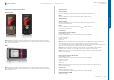
FUNCTIONAL OVERVIEW K630, V640, K660 Overview K630, V640 Technical Description SEMC Troubleshooting Manual K630 - V640 - K660 Phone memory: Up to 32 MB Memory card support: Memory Stick Micro™ (M2™) Talk time GSM: Up to 9 hrs Standby time GSM: Up to 300 hrs Talk time UMTS: Up to 5 hrs Standby time UMTS: Up to 300 hrs Networks: UMTS/HSDPA 2100 GSM/GPRS 900/1800/1900 EDGE K660 Camera 2 megapixel camera, 2.
FUNCTIONAL OVERVIEW Technical Description Connectivity Bluetooth™ technology, Modem, Synchronization, USB mass storage, USB support Baseband Part Size: 104 x 47 x 15 mm Weight: 95 grams Analog Baseband Controller Power Management N2000 (Vera) Colors: Lime on White Wine on Black Screen: 262,144 color TFT Resolution: 240 x 320 pixels Size: 2 inches Phone memory: Up to 32 MB Memory Stick Micro™ (M2™) support Talk time GSM: Up to 9 hrs Standby time GSM: Up to 330 hrs Talk time UMTS: Up to 4 hrs 30 min Sta
FUNCTIONAL OVERVIEW Functional Blocks of the Analog Baseband Controller. Technical Description SEMC Troubleshooting Manual K630 - V640 - K660 Connection Diagram FUNCTIONAL OVERVIEW 1215-3608 rev.
FUNCTIONAL OVERVIEW Technical Description SEMC Troubleshooting Manual K630 - V640 - K660 Charger Control Resistance Identification and Temperature Measurement A programmable charger is used for battery charging. Limits can be set for the output voltage at CHSENSE- and the output current from DCIO through the sense resistor to CHSENSE-. The programmable charger is enabled or disabled by the assertion/negation of the external signal DCIO.
FUNCTIONAL OVERVIEW CODEC Block Schematic Technical Description SEMC Troubleshooting Manual K630 - V640 - K660 CODEC CCO Voltage Source There is an internal voltage source CCO that provides the necessary drive current for electret microphones. The voltage source is I²C programmable to 2.2 V or 2.4 V. The source can be disabled during standby. A typical use case with a microphone connected to MIC1 and the CCO is shown in picture below.
FUNCTIONAL OVERVIEW Digital Baseband Controller (CPU) D2000 (Anja) Technical Description SEMC Troubleshooting Manual K630 - V640 - K660 Functional blocks of the Digital Baseband Controller This component is not replaceable on SL 4 because Baseband calibration is required. The Digital Baseband Controller is divided in two subsystems: - Application - Access Access Subsystem All modem functionality in the digital baseband controller resides in the Access subsystem.
FUNCTIONAL OVERVIEW Technical Description RF System Control Radio Modules The access subsystem of the digital baseband controller controls the overall radio system. In both EDGE/GSM/GPRS and WCDMA air interface mode, the digital baseband controller controls the radio system through a 3-wire serial bus. The digital baseband controller also manages PA band control and the antenna switch mechanism in the front end module.
FUNCTIONAL OVERVIEW Technical Description SEMC Troubleshooting Manual K630 - V640 - K660 The module is shielded using fence and lid technology. The main components contained are transceiver ASIC, PA module, Front End Module and X-tal. with high dynamic range. The digital output signals are sent over a serial interface to the digital base-band circuit for further processing and detection.
FUNCTIONAL OVERVIEW WCDMA Transceiver Block Diagram Technical Description SEMC Troubleshooting Manual K630 - V640 - K660 Bluetooth and FM Radio The STLC2592 circuit N1400 combines Bluetooth and FM tuner functionality into one. Bluetooth The Bluetooth implementation is compliant with Bluetooth specification 2.1 + EDR. The BluetoothTM transceiver has frequency channels with 1 MHz separation from 2402 to 2480 MHz. The same band is used for both transmission and reception. This gives 79 frequency channels.
FUNCTIONAL OVERVIEW Technical Description SEMC Troubleshooting Manual K630 - V640 - K660 System connector pin out: 1 Vbus 2 SP Ref 3 Mic+ / Aux in L 4 Mic/ Aux in R 5 Sp L / DBG TX 6 Sp R / DBG RX 7 Video / Strobe 8 AID / ACB / Vpp Flash 9 GND 10 D+ / DTMS 11 D/ DFMS 12 DCIO Clocks Clock Distribution The clocking for the access and application subsystems is separated. This means that they can wake up or go to sleep mode independently.
FUNCTIONAL OVERVIEW A B C D E N1210 SQUID MODULE WCDMA BAND I SEMC Troubleshooting Manual K630 - V640 - K660 K850 Block Diagram Access F G H I J VccA VCC1 VCC2 1 Lock Detect VDDE18 LD PA PA Bias VBATi RX PGC D2020 1Gbit NAND + 512 Mbit SDRAM D2000 ANJA DIGITAL BASEBAND CONTROLLER BUS INTERFACE SDRAM Controller 2 VCC_WPA CPU Ref CLK Static Memory Controller SDRAM Controller CLK VDDQ WE VSS CAS VSSQ RAS TXEN BA0 XGAM TXVGA BA1 PDI DAT MASTERON GSM/GPRS/EDGE Sub s
FUNCTIONAL OVERVIEW A B C D E F G D2020 1Gbit NAND 512 Mbit SDRAM VDIG VDDE18 VCORE18 1 SEMC Troubleshooting Manual K630 - V640 - K660 Block Diagram Application H LED_LCD VGA CAMERA LCD_VDIG CE VBOOST VDD RE CLE Sensor Array CLK VSS CIF_STDBY STDBY CAMRESn RESETn ALE Driver I2CDAT D(0-7) R/B Interface WE Image processing I2CCLK VCAMSD28 VCAMSD18 CAMSYSCLK Power Management MAIN CAMERA CAM_LDO_EN 2 S4300 I2CDAT I2CCLK CPU WCDMA Sub system i2CDAT Interface SDRAM Con
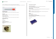
APPENDIX SEMC Troubleshooting Manual K630 - V640 - K660 Replaceable Parts Electrical Part list The list contains only components that are possible to replace on the main board. Pos. number refer to the components position number on the board. F=Front side, B=Back side. Side Pos. Description Part Number Comments Page B N1400 Module Bluetooth + FM STLC2592 1200-6182 K660 ONLY MSL3 Special Soldering Process Required - Authorized Repair Centers Only 80 B N2203 2ch-LDO, Vout1=2.8V, Vout2=1.
APPENDIX B2100 Osc. XO 32.768 kHz LC 1200-3231 SEMC Troubleshooting Manual K630 - V640 - K660 Components - B2100, B3100, L2200 B3100 Microphone RLC509429/5 L2200 Ind WW 4.7 uH +-20% 1200-0119 䇼Dimensions䇽 䇽 䇼Recommended Pad Layout䇽 䇽 㪬㪥㪠㪫㩷䋺㩷㫄㫄 APPENDIX 㪫㫆㫃㪼㫉㪸㫅㪺㪼 䋺㫧㪇㪅㪉 㪬㪥㪠㪫㩷䋺㩷㫄㫄 1215-3608 rev.
APPENDIX L2401-04 Filter 0.0 Hz 0402 REG70618/20 Dimension Components - L2401-04, N1002, N1200 SEMC Troubleshooting Manual K630 - V640 - K660 N1200 RF Module Thor 1203-6579 Equivalent Circuit 0.5±0.05 0.25±0.1 1.0±0.05 (Resistance element becomes dominant at high frequencies.) 0.5±0.05 (in mm) N1002 PA Module 22 Terminal LGA RYT101988/1 APPENDIX 1215-3608 rev.
APPENDIX N1210 RF Module Squid 1204-1674 SEMC Troubleshooting Manual K630 - V640 - K660 Components - N1210, N1400 N1400 Module Bluetooth + FM STLC2592 1200-6182 TOP VIEW BLOCK DIAGRAM AND ELECTRICAL SCHEMATIC FM _VA FM_ VD BT_H V [5: 0] BT_ VIO [4:0 ] BT_GPIO [5:0] ARM7TDMI CPU Wrapper BT_LP_CLK JTAG RECEIVER DEMOD BT_HOST_WAKEUP/ BT_SPI _INT RAM BT_RFP F I L T E R RF PLL Fractional N CONTROL AND REGISTER ROM BT _WAKEUP BT_RFN UART / SPI TRANSMITTER MOD BT _RESETN BASEBAND CORE EBC
APPENDIX N2203 2CH-LDO Vout1 = 2.8V Vout2 = 1.8V RYT113997/4 SEMC Troubleshooting Manual K630 - V640 - K660 Components - N2203, N2204, N2205 N2205 IC Vreg 1200-0107 Connection Diagrams Pin Descriptions P in # Na me A1 PV B1 V DD C1 EN C2 V CON IN D e s c r i p ti o n Power Supply Voltage Input to the internal PFET switch. Analog Supply Input. Enable Input. Set this digital input high for normal operation. For shutdown, set this pin low. Voltage Control Analog input.
APPENDIX N3100 IC Amp RYT109914/1 Components - N3100, N3101, S2400-03 SEMC Troubleshooting Manual K630 - V640 - K660 S2400-03 Input Side Switch Push RMD 10116/9 PIN CONNECTIONS 9−Pin Flip−Chip CSP A1 A2 A3 INM OUTA INP B1 B2 B3 VM_P VM Vp C1 C2 C3 BYPASS OUTB SHUTDOWN (Top View) PIN DESCRIPTION Pin Type Symbol Description A1 I INM A2 O OUTA A3 I INP B1 I VM_P B2 I VM Core Analog Ground. Positive analog supply of the cell. Range: 2.2 V−5.5 V.
APPENDIX V2202 Trans V; Dual PMOSFET RYN 122910/1 PIN D1 PINNING D2 G2 SEMC Troubleshooting Manual K630 - V640 - K660 V2420-21 Zener Diode Voltage Regulator 15V 15% RKZ223905/2 S1 G1 D2 D1 MicroFET Components - V2202, V2206, V2405, V2420-21, V3101-10, V4201 S1 1 6 D1 G1 2 5 G2 D2 3 4 S2 PIN Top view MAM387 DESCRIPTION 1 cathode 2 anode The marking bar indicates the cathode. S2 V3101-10 Zener Diode RKZ223911/1 V2206 Diode V Schottky RKZ123905/2 1.2±0.05 1.6±0.
APPENDIX X1001-03 Antenna Pin Connector SND90158 Components - X1001-03, X1200, X1201-03 SEMC Troubleshooting Manual K630 - V640 - K660 X1201-03 POGO Pin (For Antenna) SND10625 X1200 Conn Antenna RPT79947 APPENDIX 1215-3608 rev.
APPENDIX X2200 Battery Connector SND10620 Components - X2200, X2402 SEMC Troubleshooting Manual K630 - V640 - K660 X2402 Con X Keyboard Connector RNV799036 APPENDIX 1215-3608 rev.
APPENDIX X2403 SIM Card Reader SXA1096432 Components - X2403, X2490, X4200, X4310 SEMC Troubleshooting Manual K630 - V640 - K660 X4200 B to B Connector, Female 22 pin RNV799046 X4310 Conn (Camera Socket) RNV799011 X2490 MS-Micro Pico Holder RNK87147/2 APPENDIX 1215-3608 rev.
APPENDIX Components - X4300 SEMC Troubleshooting Manual K630 - V640 - K660 X4300 Conn Socket 1200-0374 APPENDIX 1215-3608 rev.
APPENDIX Troubleshooting Software Documentation SEMC Troubleshooting Manual K630 - V640 - K660 Troubleshooting Software Documentation Base Band Controls Introduction Note: Some parts of Base Band Control functions may not be implemented since they are not supported by the ITP SW. Using this software you can control most parts and functions of all Sony Ericsson mobile phones. It is a GUI (Graphical User Interface) for the commands implemented in the ITP (Integrated Test Program).
APPENDIX Equipment Setup Troubleshooting Software Documentation SEMC Troubleshooting Manual K630 - V640 - K660 Power Supply Channel 2 DCIO/SEPI Cable Connection Setup Note: The Power Supply Channel 1 (VBATT) must allow reverse current. Note: During calibration the accurate voltage from VBATT must be within ±0.015 V. If this is not fulfilled it will cause a faulty calibration. For more information about recommended power supply units, see the Repair Tool Catalogue in CSPN under the Mechanical level.
APPENDIX System Requirements Note: Before start using the Troubleshooting Software, the phone must be flashed with ITP SW. The system requirements for running the application are: Troubleshooting Software Documentation SEMC Troubleshooting Manual K630 - V640 - K660 GSM Radio Settings Used for Channel and Power Level control of the selected GSM Band. The TX and RX frequency value for selected band and channel will be presented in the TX and RX frequency box.
APPENDIX Troubleshooting Software Documentation SEMC Troubleshooting Manual K630 - V640 - K660 Fast select channels VCXO Control Set High Channel: The High Channel for selected WCDMA Band will be set by the Troubleshooting SW. Used to fine tune the VCXO to MCLK frequency by calibrating the DAC that sets the VCXO control voltage. It is also used to verify the VCXO tuning range.
APPENDIX SEMC Troubleshooting Manual K630 - V640 - K660 Examples of different FM Radio Test setups in the Troubleshooting Software Audio output: - Troubleshooting Software Documentation Earphone is the internal Earpiece speaker of the unit. AUX earphone connected to the system connector. Loudspeaker is the internal loudspeaker of the unit. OFF is used to switch off the currently used Audio Loop. Picture 11 Picture 12 Examples of different Audio Loop Test setups in Fault Trace SW.
APPENDIX Current Calibration The Current Calibration test is similar to the Current Test for the charging algorithm in the factory environment. Note: For a correct and accurate result, perform the Battery Calibration Test before current calibration. To perform this test you will need both channel 1 and 2 from the Power Supply. 1. 2. 3. 4. 5. Click 2. Current Calibration. Adjust channel 1 (the dummy battery) to 3.8 V. Click button SET VBATT to 3.8 Volt.
APPENDIX Troubleshooting Software Documentation - Camera Door Test Fault Trace SW Error Messages - Vibrator Test 1. - Keyboard Scan Test ...timeout when reading - Etc. Check the following items: Note: When one test has been deactivated the phone will be restarted. General – Tab Functions Note: Some parts of General functions may not be possible to implement for all products due to limitations in ITP Software.
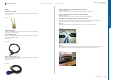
APPENDIX SEMC Troubleshooting Manual K630 - V640 - K660 Troubleshooting Fixture Setup Instructions Troubleshooting Fixture Setup Instructions Front side overview of the TRS Fixture, see picture 1. Connect Power Supply Channel 1 VBATT (Black and Red plugs) according to picture 4. Place the PBA by using Guide Pin mounted inside the TRS Fixture according to picture 7. Connect the Keypad Flex Cable to the board-toboard connector mounted on the PBA when Keypad is in use according to picture 10.
APPENDIX Troubleshooting Fixture Setup Instructions Connect Power Supply Channel 2 DCIO/SEPI Cable according to picture 13. Connect FM Radio Cable if needed according to picture 16. The Pin mounted inside the TRS Fixture marked with a RED arrow can be used as MP TRS Fixture GND or grounding for the oscilloscope probe, see picture 19. Picture 13 Picture 16 Picture 19 Secure the DCIO/SEPI Cable by using the screw according the picture 14.