
Technical data
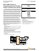

Analog Integrated Circuit Device Data
Freescale Semiconductor 9
34825
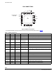
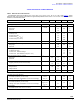
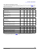
ELECTRICAL CHARACTERISTICS
STATIC ELECTRICAL CHARACTERISTICS
ID DETECTION
ID_Float Threshold
Detection threshold
V
FLOAT
- 2.3 -
V
Pull-up Current Source
When ADC result is 1xxxx
When ADC result is 0xxxx
I
ID
1.9
30.4
2.0
32
2.1
33.6
A
ID Shorted to Ground Detection
Detection current
Detection voltage threshold
I
VCBL
V
VCBL_L
1.0
-
1.2
50
1.4
-
mA
mV
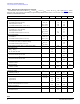
LOGIC INPUT AND OUTPUT
VDDIO Logic Input Level
Input LOW level
Input HIGH level
V
DDIO_IL
V
DDIO_IH
-
1.5
-
-
0.5
-
V
V
Push-pull Logic Output
Output HIGH level (loaded by 1.0 mA current)
Output LOW level (loaded by 4.0 mA current)
V
OH
V
OL
0.7V
DDIO
-
-
-
-
0.4
V
Open Drain Logic Output (INT)
Output LOW level (loaded by 4.0 mA current)
V
ODOL
- - 0.4
V
I
2
C INTERFACE
(7)
Low Voltage on I
2
C_SDA, I
2
C_SCL Inputs
V
I2C_IL
-0.2 - 0.3V
DDIO
V
High Voltage on I
2
C_SDA, I
2
C_SCL Inputs
V
I2C_IH
0.7V
DDIO
- V
DDIO
V
Low Voltage on I
2
C_SDA Output
V
I2C_OL
- - 0.4 V
Current Load when I
2
C_SDA Outputs Low Voltage
I
I2C_OL
0 - 4.0 mA
Leakage Current on I
2
C_SDA, I
2
C_SCL Outputs
I
I2C_LEAK
-1.0 - 1.0 A
Input Capacitance of the I
2
C_SDA, I
2
C_SCL Pins
C
I2CIN
- - 8.0 pF
Notes
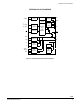
6. The OUT pin discharge MOSFET is shown in Figure 15. This MOSFET will be turned on when the power MOSFET is off.
7. These parameters are not tested. They are guaranteed by design.
Table 4. Static Electrical Characteristics (continued)
Characteristics noted under conditions V
DD
= 3.6 V, V
BUS
= 5.0 V, V
DDIO
= 3.0 V, -40 °C T
A
85 °C (see Figure 1), unless
otherwise noted. Typical values noted reflect the approximate parameter means at V
DD
= 3.6 V and T
A
= 25 °C under nominal
conditions, unless otherwise noted.
Characteristic Symbol Min Typ Max Unit