
Technical data
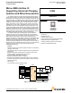

Analog Integrated Circuit Device Data
Freescale Semiconductor 7
34825
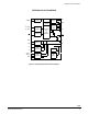
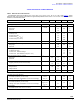
ELECTRICAL CHARACTERISTICS
STATIC ELECTRICAL CHARACTERISTICS
STATIC ELECTRICAL CHARACTERISTICS
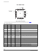
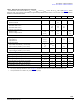
Table 4. Static Electrical Characteristics
Characteristics noted under conditions V
DD
= 3.6 V, V
BUS
= 5.0 V, V
DDIO
= 3.0 V, -40 °C T
A
85 °C (see Figure 1), unless
otherwise noted. Typical values noted reflect the approximate parameter means at V
DD
= 3.6 V and T
A
= 25 °C under nominal
conditions, unless otherwise noted.
Characteristic Symbol Min Typ Max Unit
POWER INPUT
VDD Supply Voltage
V
DD
2.7 - 5.5 V
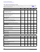
VDD Power-On-Reset Threshold
Rising edge
Hysteresis
V
VDDPOR
-
-
2.5
100
2.65
-
V
mV
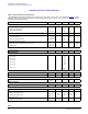
VDD Quiescent Current
In Standby mode
In Power Save mode
In Active mode (V
DD
< V
BUS
)
In Active mode (V
DD
> V
BUS
)
I
VDD
-
-
-
-
9.0
16
550
850
12
22
650
1000
A
VBUS Supply Voltage
V
BUS
2.8 5.0 28 V
VBUS Detection Threshold Voltage
Rising edge
Hysteresis
V
BUS_DET
-
-
2.65
150
2.80
-
V
mV
VBUS Supply Quiescent Current
In VBUS Power mode
In Active mode - Dedicated Charger
In Active mode - power MOSFET is off (V
BUS
< V
DD
)
I
VBUS
-
-
-
-
-
-
1.2
1.2
0.5
mA
mA
A
VBUS Overvoltage Protection Threshold
Rising edge
Hysteresis
V
BUS_OVP
6.8
-
7.0
150
7.2
-
V
mV
VBUS Overcurrent Protection Threshold
Triggering threshold (at onset of OTP shutoff)
I
BUS_OCP
1.2 1.8 2.2 A
Overtemperature Protection Threshold
Rising threshold
Falling threshold
T
OTP
115
-
130
95
145
-
°C
VDDIO Supply Voltage
V
DDIO
1.65 - 3.6 V
SWITCH
ISET Open Drain Output MOSFET
On resistance (loaded by 3.0 mA current)
Leakage current (when the MOSFET is off at 5.0 V bias voltage)
R
ISETB
I
ISET_OFF
-
-
-
-
100
0.5
A
OUT Pin Discharge MOSFET
(6)
On resistance (loaded by 3.0 mA current)
Leakage current (when the MOSFET is off at 5.0 V bias voltage)
R
OUT_DISC
I
OUT_OFF
-
-
-
0.5
100
-
A
Power MOSFET
On resistance (when V
BUS
= 5.0 V, T
A
< 50 °C)
R
PSW
- 200 250
m