
Technical data
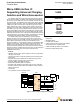


Analog Integrated Circuit Device Data
6 Freescale Semiconductor
34825
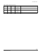
ELECTRICAL CHARACTERISTICS
MAXIMUM RATINGS
ELECTRICAL CHARACTERISTICS
MAXIMUM RATINGS
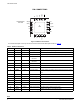
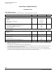
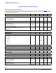
Table 3. Maximum Ratings
Exceeding these ratings may cause a malfunction or permanent damage to the device.
Ratings Symbol Value Unit
ELECTRICAL RATINGS
Input Voltage Range
VBUS Pin
OUT Pin
SPK_L, SPK_R, DP, and DM Pins
All Other Pins
V
BUS
V
OUT
-0.3 to 28
-0.3 to 8.0
-2.0 to V
DD
+0.3
-0.3 to 5.5
V
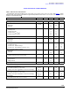
ESD Voltage
(2)
Human Body Model (HBM) for VBUS, DP, DM, ID Pins
Human Body Model (HBM) for all other pins
Machine Model (MM)
V
ESD
8000
2000
200
V
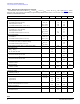
THERMAL RATINGS
Operating Temperature
Ambient
Junction
T
A
T
J
-40 to +85
150
°C
Storage Temperature
T
STG
-65 to +150
°C
Thermal Resistance
(3)
Junction-to-Case
Junction-to-Ambient
R
JC
R
JA
6.0
45
°C/W
Peak Package Reflow Temperature During Reflow
(4)
,
(5)
T
PPRT
Note 5
°C
Notes
2. ESD testing is performed in accordance with the Human Body Model (HBM) (C
ZAP
= 100 pF, R
ZAP
= 1500 ), and the Machine Model
(MM) (C
ZAP
= 200 pF, R
ZAP
= 0 ).
3. Device mounted on the Freescale EVB test board per JEDEC DESD51-2.
4. Pin soldering temperature limit is for 10 seconds maximum duration. Not designed for immersion soldering. Exceeding these limits may
cause malfunction or permanent damage to the device.
5. Freescale’s Package Reflow capability meets Pb-free requirements for JEDEC standard J-STD-020C. For Peak Package Reflow
Temperature and Moisture Sensitivity Levels (MSL), go to www.freescale.com, search by part number [e.g. remove prefixes/suffixes and
enter the core ID to view all orderable parts (i.e. MC33xxxD enter 33xxx)], and review parametrics.