
Technical data

Analog Integrated Circuit Device Data
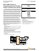
4 Freescale Semiconductor
34825
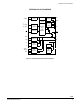
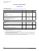
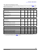
PIN CONNECTIONS
PIN CONNECTIONS
Figure 3. 34825 Pin Connections
A functional description of each pin can be found in the Functional Pin Description section on page 14.
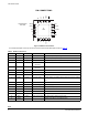
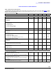
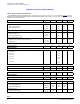
Table 2. 34825 Pin Definitions
Pin Number Pin Name Pin Function Formal Name Definition
1 SPK_R
Input Speaker right channel
Right channel input for speaker signals
2 SPK_L
Input Speaker left channel
Left channel input for speaker signals
3 MIC
Output Microphone output
Microphone output to the baseband of the cell phone system
4 D+
IO D+ of the USB
transceiver
D+ line of the USB transceiver
5 D-
IO D- of the USB
transceiver
D- line of the USB transceiver
6 RXD
Output UART receiver
Receive line of the UART
7 TXD
Input UART transmitter
Transmit line of the UART
8 NC
No Connection No Connection
No Connection
9 VDDIO
Input IO power supply
IO supply voltage. The VDDIO voltage is used as the reference voltage
for the I
2
C bus signals. This pin also functions as a hardware reset to
the IC.
10 NC
No Connection No Connection
No Connection
11 VDD
Input Power supply
IC power supply input
12 INT
Output Interrupt output
Open-drain interrupt output
13
I
2
C_SDA
IO I
2
C data
Data line of the I
2
C interface
14
I
2
C_SCL
Input I
2
C clock
Clock line of the I
2
C interface
15 OUT
Output Power output
The output of the power MOSFET pass switch
16 ISET
Output Charge current setting
Open-drain output to set the charger current
17 VBUS
Input VBUS power supply
VBUS line of the Mini or micro-USB connector
TRANSPARENT
TOP VIEW
SPK_R
SPK_L
MIC
D+
D-
RXD
TXD
NC
VDDIO
NC
VDD
INT
I
2
C_SDA
I
2
C_SCL
OUT
ISET
VBUS
DM
DP
ID
GND
1
2
3
4
5
678910
11
12
13
14
15
1617181920
21