
Technical data


Analog Integrated Circuit Device Data
Freescale Semiconductor 31
34825
FUNCTIONAL DEVICE OPERATION
REGISTER MAP
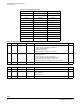
Table 18. Status Register
Bit Mode Symbol Reset Description Notes
0
R ADC_Status x
ADC conversion status
1: ADC conversion completed
0: ADC in progress
1
R VBUS_DET x
VBUS voltage is higher than the POR
0: no
1: yes
2
R ID_FLOAT x
ID line is floating
0: no
1: yes
3
R ID_GND 0
ID pin is shorted to ground
0: no
1: yes
4
R DP/DM_SHORT 0
DP/DM shorted
0: no
1: yes
5
R USB_CHG 0
A USB charger is connected
0: no
1: yes
6
R FET_STATUS x
The on/off status of the power MOSFET
0: off
1: on
7
R Reserved 0
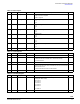
Table 19. Control Register
Bit Mode Symbol Reset Description Notes
1-0
R/W Reserved x0
2
W/C RESET 0
Soft reset. When written to 1, the IC is reset. Once the reset is complete,
the RST bit is set and the RESET bit is cleared automatically.
1: to soft reset the IC
4-3
R/W Reserved 00
5
R/W AutoPSAVE 1
Automatic Power Save mode detection control
0: disable automatic Power Save mode detection. Device can enter Power
Save mode via the I
2
C
1: enable automatic Power Save mode detection.
7-6
R/W Reserved 01
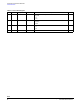
Table 20. Time Delay Register
Bit Mode Symbol Reset Description Notes
3-0
R/W TD 0100
Time delay to start the powered accessory identification flow after
detecting the VBUS voltage
0000: 100 ms
0001: 200 ms
0010: 300 ms
0011: 400 ms
0100: 500 ms
......
1111:1600 ms
7-4
R/W Reserved 1001