
Technical data

Analog Integrated Circuit Device Data
30 Freescale Semiconductor
34825
FUNCTIONAL DEVICE OPERATION
REGISTER MAP
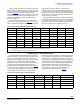
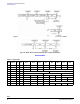
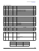
0011 400 ms 600 ms
0100 500 ms 700 ms
0101 600 ms 800 ms
0110 700 ms 900 ms
0111 800 ms 1000 ms
1000 900 ms 1100 ms
1001 1000 ms 1200 ms
1010 - 1300 ms
1011 - 1400 ms
1100 - 1500 ms
1101 - -
1110 - -
1111 - -
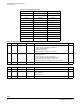
Table 16. S/W Control Register 1
Bit Mode Symbol Reset Description Notes
1-0
R/W VBUS Switching 01
VBUS line switching configuration
00: open all switches connected to the VBUS line.
01: internal power MOSFET on
10: VBUS connected to MIC
11: open all switches connected to the VBUS line.
4-2
R/W DP/DM Switching 000
DP/DM line switching configuration
000: open all switches
001: DP connected to D+, DM connected to D-
010: DP connected to SPK_R, DM connected to SPK_L
011: DP connected to RxD, DM connected to TXD
Others: open all switches connected to the DP pin and DM pin
7-5
R Reserved 000
Table 17. S/W Control Register 2
Bit Mode Symbol Reset Description Notes
3-0
R/W Reserved 0100
4
R/W ISETB 0
ISET output
0: high-impedance
1: low-impedance
7-5
R/W Reserved 000
Table 15. Timing Table (continued)
Setting Value Key Press Long Key Press