
Technical data
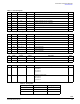

Analog Integrated Circuit Device Data
Freescale Semiconductor 27
34825
FUNCTIONAL DEVICE OPERATION
I2C SERIAL BUS INTERFACE
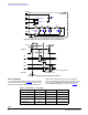
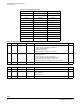
Figure 21. Hardware Reset Using the VDDIO Input
INTERRUPT
There are eight interrupt sources in the 34825 causing an
interrupt at the INT pin to the host IC. They are accessory
attachment, accessory detachment, short-key press, long
key press, long-pressed key release, VBUS voltage OVP, the
IC temperature OTP, and either the OVP or the OTP
condition is removed. The 34825 detects each event and sets
the corresponding bit in the Interrupt register. As long as the
Interrupt register is set, the
INT pin outputs low voltage. The
Interrupt register is not writable. When the Interrupt register is
read, the Interrupt register is cleared automatically. Once the
Interrupt register is cleared, the
INT pin returns to high
voltage.
An interrupt mask register is provided to mask unwanted
interrupt source. When the bit of the Interrupt Mask register
is set to 1, the corresponding interrupt source is blocked. The
INT does not output low voltage even though this interrupt bit
is set in the Interrupt register.
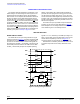
LOGIC OUTPUT
There are two open-drain logic output pins, INT and ISET.
The
INT pin is related to the interrupt sources as described in
the Interrupt section. The ISET pin is controlled by the
register bit with the same name in the Control register.
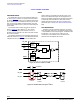
The ISET generally is used to control the charge current
level. A typical charger IC uses one external resistor to set
the charge current. By using
ISET output, the charger IC can
use two external resistors in parallel to set two charge current
levels, as shown in
Figure 27.
I
2
C SERIAL BUS INTERFACE
The I
2
C bus is enabled in the Standby, the Power Save,
and the Active modes. The serial clock (SCL) and the serial
data (SDA) lines must be connected to a positive supply
using pull-up resistors. Internally the I
2
C bus voltage is
referenced to the VDDIO input. The 34825 is a slave device.
Maximum data rate is 400
kbps.
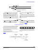
ADDRESSING AND PROTOCOL
The 7-bit address for the 34825 is 0100101, as shown in
Figure 22.
Figure 22. I
2
C Slave Address
The following three figures show three I
2
C-bus transaction
protocols. The Word Address is an 8-bit register address in
the 34825.
Figure 23. Master Transmits to Slave (Write Mode)
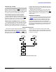
VDDIO
Reset
t
VDDIODGT_F
0
1
0
0
101
R/W