
Technical data

Analog Integrated Circuit Device Data
26 Freescale Semiconductor
34825
FUNCTIONAL DEVICE OPERATION
LOGIC CONTROL FEATURES
LOGIC CONTROL FEATURES
RESET
HARDWARE RESET
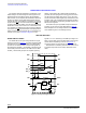
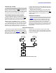
The 34825 has three sources for hardware resetting the
IC. As the
Figure 19 shows, the sources include the Power-
On-Reset caused by the rising V
DD
, a hardware reset caused
by the VDDIO input and a hardware reset using the I
2
C bus
lines. The Power-On-Reset is described earlier. The reset
caused by the VDDIO input or by the I
2
C bus lines belongs to
system resets.
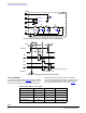
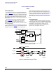
The hardware reset condition using the I
2
C signals is
shown in Figure 20. When both the I
2
C_SCL and the
I
2
C_SDA have a negative pulse with time of t
RSTI2C
, a
hardware reset is generated. The result of the reset is same
as a Power-On-Reset.
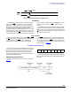
The operating waveforms of the hardware reset using the
VDDIO pin are shown in Figure 21. The VDDIO detection has
a deglitch-time t
VDDIODGT_F
. A glitch on the VDDIO with
duration less than the deglitch time will be ignored. If the
pulse on the VDDIO lasts longer than the deglitch time, a
reset from the VDDIO is detected to generate a reset signal.
To effectively reset the 34825, the reset pulse from the
VDDIO needs be longer than the 150
s minimum reset
pulse width given in the
Dynamic Electrical Characteristics
table.
SOFTWARE RESET
In addition to the two hardware reset types, the system
reset has another reset source, the software reset by writing
‘1’ to the RESET bit in the Control register. The Reset bit will
be cleared to ‘0’ at once since it is of W/C type. The
consequence of the software reset is the same as the
hardware reset. All registers will be reset.
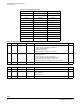
Figure 19. Sources of Reset in 34825
Figure 20. Hardware Reset Using the I
2
C Bus
reset
+
-
V
VDDPOR
VDD
I
2
C_SDA
I
2
C-Bus
Reset
Detection
Delay
Time
I
2
C_SCL
VDDIO
VDDIO
Reset
Detection
I2C_SDA
I2C_SCL
Reset
Condition
Start
Condition
Stop
Condition
Reset
8.8~13.5ms