
Technical data
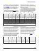

Analog Integrated Circuit Device Data
Freescale Semiconductor 23
34825
FUNCTIONAL DEVICE OPERATION
OPERATION AFTER IDENTIFICATION
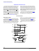
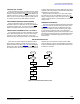
POWER MOSFET
The SW8 in Figure 15 is a power MOSFET that controls
the power flow from the VBUS input to the OUT pin. The
power MOSFET serves two purposes. For the Audio
accessory with microphone, the power MOSFET isolates the
VBUS pin from both the input decoupling capacitor and the
input quiescent current of the charger IC connected to the
OUT pin, so that the microphone signal can be connected to
the VBUS pin without any interference from the OUT pin. The
power MOSFET is also used as the input overvoltage
protection (OVP) or overcurrent protection (OCP) switch for
other components in the cell phone, such as the charger IC,
to allow a low voltage rated charger IC to be used for cost
reduction.
The power MOSFET is guaranteed to be turned on in
VBUS power mode even when the VDD voltage is below
V
VDDPOR
threshold, to ensure that the cell phone battery can
be charged when the battery is fully discharged.
PROTECTION
OVERVOLTAGE PROTECTION (OVP)
The VBUS line is capable of withstanding a 28 V voltage.
The 34825 protects the cell phone by turning off the internal
power MOSFET when the VBUS voltage is higher than the
OVP threshold. In this case, the 34825 turns off the power
MOSFET within 1.0
s after the input voltage exceeds the
OVP threshold, and the OVP_EN bit in the Interrupt register
is set to interrupt the host IC. When the OVP event is cleared,
the OVP_OTP_DIS bit in the Interrupt register is set to inform
the host IC.
OVERCURRENT PROTECTION (OCP) AND
OVERTEMPERATURE PROTECTION (OTP)
If the current flowing through the power MOSFET exceeds
the specified OCP limit, the 34825 will operate in CC
(constant current) mode, regulating the output current at the
OCP limit. If the OCP condition persists, the IC temperature
will rise, eventually reaching the overtemperature protection
(OTP) limit. The 34825 then turns off the power MOSFET and
sets the OTP_EN interrupt bit in the Interrupt register to
inform the host IC. The power MOSFET is turned on again
when the IC temperature falls below the OTP falling
temperature threshold, and the OVP_OTP_DIS bit is set. If
the above case happens repeatedly seven times, the power
MOSFET will be permanently turned off until the accessory is
detached or the IC is reset.
The power MOSFET is turned off with a limited speed
under the OTP case to prevent a high overshoot voltage at
the VBUS pin.
OPERATION WITH ACCESSORIES
AUDIO ACCESSORY SUPPORTING REMOTE
CONTROLLER (R/C ACCESSORY)
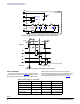
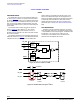
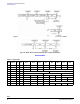
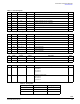
Two ID resistors are designated for accessories with a
remote controller, as listed in Table 22. A typical accessory
with a remote controller is an audio headset that has a stereo
speaker, a micro phone, and a remote controller, as shown in
Figure 16. The five pins in the mini or micro-USB connector
are assigned in Figure 16. If some components are not
included in the accessory, the corresponding pins should be
left floating. For example, if the microphone is not included in
the stereo headset, VBUS pin should be left floating in the
headset.
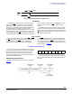
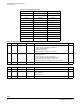
The timing of the key pressing is shown in Figure 17. If a
key is pressed for a time less than 20 ms, the 34825 ignores
this key press. If the key is still pressed after 20
ms, 34825
starts a timer to count the time during which the key is
pressed. There are three kinds of key press conditions
according to the pressing time: error key press, short key
press, and long key press.
1. Error key press: if the key pressing time is less than
T
KP
, The 34825 ignores this key press.
2. Short key press: if the key pressing time is between
T
KP
and T
LKP
, the KP bit is set to inform the host IC.
The ADC result holds the key value. The
INT outputs
low impedance when the key is released and returns to
a high -mpedance, due to the clearance of the KP bit
when the interrupt register is read.
3. Long key press: if the key pressing time is longer than
T
LKP
, the long key press bit LKP in the Interrupt register
is set to inform the host IC. The host IC needs to
respond to the key press immediately. The ADC result
holds the key value. When the key is released, the long
key release bit LKR in the Interrupt register is set to
interrupt the host IC again. The ADC Result register
still has the key value.
When such a accessory is attached, the 34825 can either
be forced into the Power Save mode or automatically enter
into the Power Save mode. This is controlled by the
AutoPSAVE bit in the Control register.
When AutoPSAVE = 1, if no activity is detected at the
SPK_L and SPK_R pins in 10 seconds, the 34825 enters the
Power Save mode automatically to minimize the quiescent
current. Upon detecting the activity in audio signal switches,
the 34825 returns to the Active mode. When AutoPSAVE = 0,
the host IC can control the mode of 34825 manually by
setting the PSAVE bit in the Device Mode register via I
2
C.
In the Power Save mode, the key pressing is monitored as
well.