
Technical data

Analog Integrated Circuit Device Data
22 Freescale Semiconductor
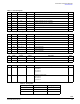
34825
FUNCTIONAL DEVICE OPERATION
OPERATION AFTER IDENTIFICATION
OPERATION AFTER IDENTIFICATION
The operation after the identification is dependent on the
VDDIO voltage. The VDD voltage has to be higher than its
POR threshold for the 34825 to perform the identification
state machine. Once completed, the identification results are
stored in the Status and the ADC Result registers and the
ATTACH bit is set. If the VDDIO is not powered, the interrupt
signal from the
INT pin cannot be sent because the INT pin is
normally pulled up to the VDDIO. The host cannot access the
34825 either via the I
2
C bus. Hence, no communication will
occur between the 34825 and the host IC when the VDDIO is
not powered. The INT signal will send an interrupt signal if the
VDDIO is powered and the ATTACH bit is not masked by the
ATTACH_m bit (refer to
Interrupt on page 27 for more
details). If the ATTACH bit is masked while the VDDIO is
powered, the interrupt signal will not be sent but the host IC
can still access the register map via the I
2
C bus. Once the
host IC accesses the 34825 register map and determines the
accessory type, it can manage the analog switches and other
signals in the 34825 by programming the S/W Control 1 and
S/W Control 2 registers.
The switches are open by default except if the attached
accessory is one of the four test cables listed in Table 22.
More descriptions on the analog switches and the operation
of the 34825 are given in the following sections.
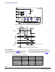
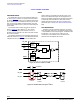
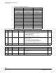
ANALOG SWITCHES
SIGNAL SWITCH ARRAY
The 34825 offers an array of analog switches for signal
switching, as shown in Figure 15. Two pairs of switches (USB
and UART) are for switching the UART and USB signals to
the micro or mini-USB connector. Stereo audio signals can
be switched from the SPK_L and the SPK_R inputs to the DP
and the DM pins that are wired to the USB connector. Both
the SPK_L and the SPK_R inputs are capable of passing
signals of +/-1.5 V, referencing to the GND pin voltage. The
SPK_L and the SPK_R pins are pulled down to ground via a
100
k resistor respectively, as shown in Figure 15. A
microphone switch connects the MIC pin to the VBUS pin.
All switches are controlled by bits in the S/W Control 1 and
2 registers except when the accessory attached is a test
cable.
Figure 15. Analog and Digital Switches
SPK_R
SPK_L
MIC
DP
DM
VBUS
RXD
TXD
D+
D-
SW2
SW1
SW3
SW4
SW6
SW7
SW5
OUT
SW8
SW9
SW10
ISET
Gate
Drive