
Technical data

Analog Integrated Circuit Device Data
18 Freescale Semiconductor
34825
FUNCTIONAL DEVICE OPERATION
POWER-UP
detecting audio signal activities or an accessory detachment.
If the transition is caused by an accessory detachment, the
34825 moves from the Power Save mode to the Standby
mode directly. Otherwise, it moves to the Active mode, and
the configuration of the IC resumes to the same configuration
before entering the Power Save mode.
DEVICE MODE REGISTER
The PSAVE bit, ACTIVE bit and RST bit in the Device
Mode register (refer to Table 10) hold the information of the
device operational mode. The RST bit, which is of R/C (read
and clear) type, indicates whether a reset has occurred. The
RST bit is set when a reset occurs (refer to
Reset for more
information). The RST bit is cleared when read by an I
2
C
access. The ACTIVE bit and the PSAVE bit together indicate
the device mode by the relationship shown in
Table 6. When
the device is in the VBUS Power mode, the registers are not
powered up.
The ACTIVE bit is a R/W (read and write) bit, it can be
written by an I
2
C operation. When the host IC writes ‘0’ to the
ACTIVE bit, the device will be forced to the Standby mode. If
an accessory is attached when the ACITVE is set to 0, the
accessory identification flow shown in Figure 14 will be re-
started.
The PSAVE bit is also a R/W bit. When the 34825 is
configured to the Auto Power-save mode (AutoPSAVE bit is
set to 1), the PSAVE bit indicates whether the 34825 is in the
Power Save mode or not. When the 34825 is configured to
the Manual Power-save mode (AutoPSAVE bit set to 0), the
host IC can writes ‘1’ to the PSAVE bit to force the 34825 into
the Power Save mode when an Audio R/C accessory is
attached. For all other accessories attachment, the 34825
does not enter the Power Save mode even the PSAVE bit is
set to 1.
POWER-UP
The 34825 has four possible power-up scenarios
depending on which of the VDD pin and the VBUS pin is
powered up first. The four scenarios correspond to the
following four mode transitions.
1. From Power Down to VBUS Power: the VBUS pin is
powered up when V
DD
< V
VDDPOR
(VDD POR
threshold)
2. From VBUS Power to Standby: VBUS is already
powered when the VDD voltage rises above its POR
threshold
3. From Power Down to Standby: the VDD pin is
powered up when V
BUS
< V
VBUSPOR
(VBUS POR
threshold)
4. From Standby to Active: the VDD pin is already
powered when the VBUS voltage rises above its POR
threshold
SCENARIO 1: VDD = 0 V AND VBUS IS POWERED
UP (POWER DOWN MODE TO VBUS POWER
MODE TRANSITION)
If the VDD pin is not powered but the VBUS is powered up
within a voltage range between the POR threshold and the
OVP (overvoltage protection) threshold, the internal power
MOSFET is softly turned on. The IC is in the VBUS Power
mode.
In this VBUS Power mode, the ISET outputs high-
impedance and all registers are in the reset state. The power
MOSFET remains on unless it is disabled by the overvoltage
protection or the overtemperature protection block.
SCENARIO 2: VBUS = HIGH AND VDD IS
POWERED UP (VBUS POWER MODE TO STANDBY
MODE TRANSITION)
If the VBUS pin is already powered when the VDD pin is
powered up, the device moves from the VBUS Power mode
to the Standby mode and then quickly moves to the
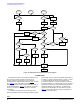
identification flow of the Active mode to identify the
accessory, as shown in
Figure 14.
After the VDD pin is powered up, the 34825 starts up the
internal supplies. The POR resets all register bits. The power
MOSFET remains on during the reset process.
SCENARIO 3: VBUS = 0 V AND VDD IS POWERED
UP (POWER DOWN MODE TO STANDBY MODE
TRANSITION)
If no accessory is plugged into the micro or mini-USB
connector when VDD is powered up, the 34825 moves from
the Power Down mode to the Standby mode. The internal
supplies are started up first, and then the whole chip is reset
and is ready to accept accessories. Then when an accessory
is attached, the 34825 enters the Active mode. The power
MOSFET is off in this case since VBUS = 0
V.
SCENARIO 4: VDD = HIGH AND VBUS IS
POWERED UP (STANDBY TO ACTIVE MODE
TRANSITION)
This is a normal VBUS detection case as shown in
Figure 14. More description can be found in Power Supply
Type Identification.
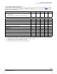
Table 6. The Device Modes vs. the Register Bits
PSAVE ACTIVE MODE
0 0 Standby
0 1 Active
1 1 Power Save
1 0 Undefined