
Technical data
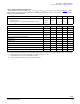

Analog Integrated Circuit Device Data
16 Freescale Semiconductor
34825
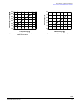
FUNCTIONAL DESCRIPTION
FUNCTIONAL INTERNAL BLOCK DESCRIPTION
FUNCTIONAL INTERNAL BLOCK DESCRIPTION
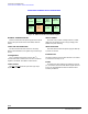
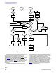
Figure 12. 34825 Functional Internal Block Diagram
INTERNAL POWER SUPPLIES
This block contains the bias power supplies to the internal
circuits. The inputs to this block include VBUS, VDD and
VDDIO.
LOGIC AND STATE MACHINE
This block includes the state machine for accessory
detection and identification, the register map, and other logic
circuits.
I
2
C INTERFACE
The I
2
C interface block has the circuit for the I
2
C
communication that a master device can use to access the
registers in the 34825. The 34825 is a slave device.
LOGIC OUTPUT
The logic output includes two open-drain logic output
signals, INT and ISET.
SWITCH ARRAY
The switch array consists of analog switches for UART,
USB, audio signal switching and one high-voltage power
MOSFET for power switching.
VBUS DETECTION
This block detects whether the power supply at VBUS pin
is present or removed.
ID DETECTION
This block contains a circuit to detect whether an ID resistor
is connected to the ID pin or not.
ID ADC
An internal 5-bit ADC measures the resistance at the ID
pin. The result is stored in the ADC Result register and sent
to the Logic and State Machine block to determine what
accessory is attached.
Switch
Array
I
2
C
Interface
VBUS
Detection
Logic
Output
Internal
Power
Supplies
Logic &
State
Machine
ID ADC
ID
Detection