
Technical data

Analog Integrated Circuit Device Data
14 Freescale Semiconductor
34825
FUNCTIONAL DESCRIPTION
INTRODUCTION
FUNCTIONAL DESCRIPTION
INTRODUCTION
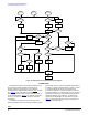
The 34825 is designed to support cell phones that adopt
the micro or mini-USB connector as the sole wired interface
between the cell phone and external accessories. Using the
micro-USB connector for charging and USB data
communication is required by the OMTP standard for the
UCS. The 34825 further extends the micro-USB connector to
support other accessories to eliminate all other mechanical
connectors in a cell phone. The supported accessories
include various audio headsets, UART connection, R/D test
cables for firmware downloading, and other user defined
accessories, in addition to the chargers defined in the Battery
Charging Specification, Revision 1.0, from the USB
Implementer’s Forum and the CEA-936-A USB Carkit
Specification, from the Consumer Electronics Association
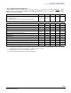
(CEA). The supported chargers are listed in
Table 8.
The 34825 offers two mechanisms to assist the
identification of the accessory. The ID detection mechanism
allows the cell phone to measure the ID resistor value
between the ID pin and the ground with a 5-bit ADC. The
VBUS detection mechanism allows the cell phone to find out
the connection status between the D+ and D- pins. Together,
the exact accessory can be determined. A detection flow is
initiated by a change in the VBUS pin voltage or by a change
in the ID pin floating status. Detaching the accessory from the
micro or mini-USB connector causes the VBUS voltage or/
and the ID resistance to change. The identification flow will be
initiated to confirm if an accessory is still connected. The host
can also initiate the identification flow by resetting an ACTIVE
bit in the register from 1 to 0.
Upon the completion of the identification flow, an interrupt
signal is sent to the host IC, so the host IC can take further
actions. The 34825 contains switches that the host IC can
control via an I
2
C interface. Based on the accessory, the host
IC can configure the switch connections in the 34825, so that
the signal paths for the USB communication, or the UART
communication, or audio accessories can be established
between the micro or mini-USB connector pins and the
system ICs. If the accessory is a power supply, the supplied
voltage is switched to the Li-ion battery charging function in
the cell phone via an internal power MOSFET.
The host IC controls the 34825 via the I
2
C serial bus. The
register map in the 34825 contains status information of the
device and the control bits that the host IC can access to
control the 34825.
FUNCTIONAL PIN DESCRIPTION
SPEAKER RIGHT CHANNEL (SPK_R)
Right channel of the baseband speaker output.
SPEAKER LEFT CHANNEL (SPK_L)
Left channel of the baseband speaker output.
MICROPHONE OUTPUT (MIC)
Microphone output to the baseband.
D+ OF THE USB TRANSCEIVER (D+)
D+ line of the USB transceiver.
D- OF THE USB TRANSCEIVER (D-)
D- line of the USB transceiver.
UART RECEIVER (RXD)
Receiver line of the UART.
UART TRANSMITTER (TXD)
Transmitter line of the UART.
NO CONNECT (NC)
These pins are not used in application. Freescale
recommends that these pins be floated
IO POWER SUPPLY (VDDIO)
Power supply input for the logic IO interface. Generally the
IO power supply voltage should be the same as the IO
voltage used in the cell phone system. VDDIO is also one of
the hardware reset input sources. A falling edge at this pin will
reset the 34825. See
Reset for more information.
POWER SUPPLY (VDD)
Power supply input. Bypass to ground with a 1.0 F
capacitor.
INTERRUPT OUTPUT (INT)
Active low open-drain output. The INT pin sends an
interrupt signal to the host IC when an interrupt event
happens. The INT output returns to high voltage once all
interrupt bits are read.
DATA LINE OF THE I
2
C INTERFACE (I
2
C_SDA)
Data line of the I
2
C interface.
I
2
C CLOCK (I
2
C_SCL)
Clock line of the I
2
C interface. The I
2
C_SCL input together
with the I
2
C_SDA input forms one of the hardware reset input
sources.