
Technical data

Analog Integrated Circuit Device Data
Freescale Semiconductor 11
34825
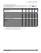
ELECTRICAL CHARACTERISTICS
DYNAMIC ELECTRICAL CHARACTERISTICS
I
2
C Reset Timing
I
2
C reset pulse width
I
2
C_SDA/I
2
C_SCL concurrent low time without causing a reset
t
RSTI2C
t
NRSTI2C
13.5
-
-
-
-
8.8
ms
I
2
C INTERFACE
(10)
SCL Clock Frequency
f
SCL
- - 400 kHz
Bus Free Time between a STOP and START Condition
t
BUF
1.3 - - s
Hold Time Repeated START Condition
t
HD:STA
0.6 - - s
Low Period of SCL Clock
t
LOW
1.3 - - s
High Period of SCL Clock
t
HIGH
0.6 - - s
Setup Time for a Repeated START condition
t
SU:STA
0.6 - - s
Data Hold Time
t
HD:DAT
0.0 - - s
Data Setup Time
t
SU:DAT
100 - - ns
Rising Time of Both SDA and SCL Signals
t
R
20+0.1C
B
- - ns
Falling Time of Both SDA and SCL Signals
t
F
20+0.1C
B
- - ns
Setup Time for STOP Condition
t
SU:STO
0.6 - - s
Input Deglitch Time (for Both Rising and Falling Edges)
t
DGT
55 - 300 ns
Notes
8. The protection delay is defined as the interval between VBUS voltage rising above the OVP rising threshold, and the OUT pin voltage
dropping below the OVP rising threshold voltage for a VBUS ramp rate of >1.0
V/s.
9. The OVP deglitch timer is only for the falling edge threshold.
10. These parameters are not tested. They are guaranteed by design.
Table 5. Dynamic Electrical Characteristics
Characteristics noted under conditions V
DD
= 3.6 V, V
BUS
= 5.0 V, V
DDIO
= 3.0 V, -40°C T
A
85°C (see Figure 1), unless
otherwise noted. Typical values noted reflect the approximate parameter means at V
DD
= 3.6 V and T
A
= 25°C under nominal
conditions, unless otherwise noted.
Characteristic Symbol Min Typ Max Unit