
Technical data
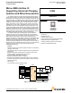

Analog Integrated Circuit Device Data
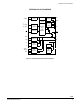
10 Freescale Semiconductor
34825
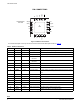
ELECTRICAL CHARACTERISTICS
DYNAMIC ELECTRICAL CHARACTERISTICS
DYNAMIC ELECTRICAL CHARACTERISTICS
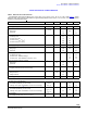
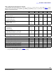
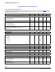
Table 5. Dynamic Electrical Characteristics
Characteristics noted under conditions V
DD
= 3.6 V, V
BUS
= 5.0 V, V
DDIO
= 3.0 V, -40 ° C T
A
85°C (see Figure 1), unless
otherwise noted. Typical values noted reflect the approximate parameter means at V
DD
= 3.6 V and T
A
= 25°C under nominal
conditions, unless otherwise noted.
Characteristic Symbol Min Typ Max Unit
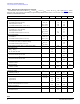
POWER ON AND OFF DELAY
VDD Power-On-Reset Timing
VDD rising deglitch time
VDD falling deglitch time
t
D2
t
VDDDGT_F
7.0
1.7
8.5
2.5
10.2
3.5
ms
VBUS Detection Deglitch Time (for Both Rising and Falling Edges)
(10)
t
VBUS_DET
3.5 4.5 5.7 ms
VBUS Overvoltage Protection
Protection delay
(8)(10)
Falling edge deglitch time
(9)
t
OVPD
t
OVPDGT_F
-
-
-
25
2.0
-
s
VBUS Overtemperature Protection
MOSFET turning off speed when OTP occurs
(10)
Deglitch time
t
OTP_TO
t
OTP_DGT
-
-
-
15
0.5
-
A/s
s
OSCILLATOR
Oscillation Frequency
f
OSC
85 100 112 kHz
SWITCHING DELAY
ID Detection Delay Time after VBUS Applied (Default Value is TD = 0100)
TD = 0000
TD = 0001
TD = 0010
TD = 0011
TD = 0100
......
TD = 1111
t
D
-
-
-
-
-
......
-
100
200
300
400
500
......
1600
-
-
-
-
-
......
-
ms
ID DETECTION
ID Float Detection Deglitch Time
t
ID_FLOAT
- 20 - ms
ID Shorted to Ground Detection Time (The Detection Current Source On Time)
t
VCBL
- 20 - ms
ADC
ADC Conversion Time
t
CONV
- 1.0 - ms
REMOTE CONTROL
Key Press Comparator Debounce Time
t
RMTCON_DG
- 20 - ms
RESET TIMING
Device Reset Time
t
RSTDVC
- 10 - s
VDDIO Logic Input Timing
Rising edge deglitch time
Falling edge deglitch time
t
VDDIODGT_R
t
VDDIODGT_F
660
105
875
125
1130
150
s
VDDIO Reset Timing
VDDIO reset pulse width
t
RSTVDDIO
150 - -
s