
User Manual

Smart Machine Smart Decision
SIM7100_Hardware_Design_V1.02 2015-06-16
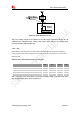
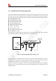
Figure 32: ISINK Reference Circuit
Note: The sinking current can be adjusted to meet the design requirement through the AT
command “AT+ CLEDITST =<0>, <value>”.The “value” ranges from 0 to 8, on behalf of the
current from 0mA to 40mA by 5mA step.
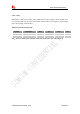
3.14.2 ADC
SIM7100 has 2 dedicated ADC pins named ADC1 and ADC2.They are available for digitizing
analog signals such as battery voltage and so on. These electronic specifications are shown in the
following table.
Table 22: ADC1 and ADC2 Electronic Characteristics
Characteristics
Min. Typ. Max. Unit
Resolution
–
15
–
Bits
Conversion time
–
442
–
ms
Input Range
0.3
VBAT
V
Input serial resistance 1
– –
MΩ
Note: “AT+CADC” and “AT+CADC2” can be used to read the voltage of the ADC1 and ADC2
pins, for more details, please refer to document [1].