
User Manual
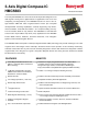

HMC5883
www.honeywell.com 5
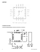
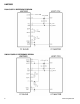
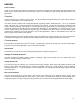
MOUNTING CONSIDERATIONS
The following is the recommend printed circuit board (PCB) footprint for the HMC5883.
PCB Pad Definition and Traces
The HMC5883 is a fine pitch LCC package with a 0.50mm pin pitch (spacing), with the pin pads defined as 0.325mm by
0.25mm in size. PCB pads are recommended to be oversized by 0.025mm from each pad for a short dimension oversize
of 0.05mm. The interior PCB pad is recommended to be 0.05mm oversized per pin with an exterior oversize of 0.20mm
for proper package centering and to permit test probing. Size the traces between the HMC5883 and the external
capacitors (C1 and C2) to handle the 1 ampere peak current pulses with low voltage drop on the traces.
Stencil Design and Solder Paste
A 4 mil stencil and 100% paste coverage is recommended for the electrical contact pads.
Pick and Place
Placement is machine dependant and no restrictions are recommended, and have been tested with mechanical centering.
Placement force should be equivalent 1206 SMT resistors and enough force should be used to squeeze the paste out
from the package/contact pad overlap and to keep the package pin contacts vertical.
Reflow Assembly
This device is classified as MSL 3 with 260 C peak reflow temperature. A baking process (125 C, 24 hrs) is required if
device is not kept continuously in a dry (< 10% RH) environment before assembly. No special reflow profile is required for
the HMC5883 which is compatible with lead eutectic and lead-free solder paste reflow profiles. Honeywell recommends
the adherence to solder paste manufacturer’s guidelines.
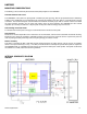
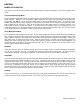
INTERNAL SCHEMATIC DIAGRAM
HMC5883