
Data Sheet

7
MachXO2 Breakout Board
Evaluation Kit User’s Guide
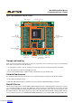
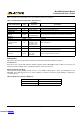
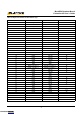
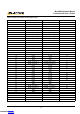
Table 1 describes the components on the board and the interfaces it supports.
Table 1. Breakout Board Components and Interfaces
Component/Interface Type
Schematic
Reference Description
Circuits
USB Controller Circuit U2: FT2232H USB-to-JTAG interface and dual USB UART/FIFO IC
USB Mini-B Socket I/O J7:USB_MINI_B Programming and debug interface
Components
LCMXO2 FPGA
U3: LCMXO2-
7
000HE-4TG144C
7000-LUT device packaged in a 20 x 20mm, 144-pin TQFP
Interfaces
LED Array Output D8-D1 Red LEDs
Four 2x20 Header
Landings
I/O
J2: header_2x20
J3: header_2x20
J4: header_2x20
J5: header_2x20
User-definable I/O
1x8 Header Landing I/O J1: header_1x8 Optional JTAG interface
4x15 60-Hole Prototype
Area
Prototype area 100mil centered holes.
Test Points Power
TP1: +3.3V
TP2: +1.2V
TP3: GND
Power and ground reference points
Subsystems
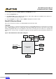
This section describes the principle sub systems for the Breakout Board in alphabetical order.
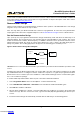
Clock Sources
All clocks for the counter demonstration des
igns originate from the MachXO2 on-chip oscillator. You may use an
expansion header landing to drive a FPGA input with an external clock source.
Expansion Header Landings
The expansion header landings provide access to user GPIOs, primary inputs, clocks, and VCCO pins of the
M
achXO2. The remaining pins serve as power supplies for external connections. Each landing is configured as
one 2x20 100 mil.
Table 2. Expansion Connector Reference
Item Description
Reference Designators J2, J3, J4, J5
Part Number header_2x20
Downloaded from Arrow.com.Downloaded from Arrow.com.Downloaded from Arrow.com.Downloaded from Arrow.com.Downloaded from Arrow.com.Downloaded from Arrow.com.Downloaded from Arrow.com.