MachXO2 Breakout Board Evaluation Kit User’s Guide January 2014 Revision: EB68_02.2 Downloaded from Arrow.com.
MachXO2 Breakout Board Evaluation Kit User’s Guide Introduction Thank you for choosing the Lattice Semiconductor MachXO2™ Breakout Board Evaluation Kit! This user’s guide describes how to start using the MachXO2 Breakout Board, an easy-to-use platform for evaluating and designing with the MachXO2 ultra-low density FPGA. Along with the board and accessories, this kit includes a pre-loaded demonstration design. You may also reprogram the on-board MachXO2 device to review your own custom designs.
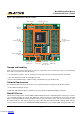
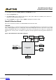
MachXO2 Breakout Board Evaluation Kit User’s Guide Figure 1. MachXO2 Breakout Board, Top Side LED Array (J4) 4x15 60-Hole Prototype Array (J6) MachXO2 PLD (U3) Two 2x20 Header Landings (J2, J4) Two 2x20 Header Landings (J3, J5) FTDI USB to UART/FIFO IC (U1) JTAG Header Landing (J1) USB Mini-B Socket (J7) Power/GND Power LED Test Points (PWR_ON) (TP1, TP2, TP3) Storage and Handling Static electricity can shorten the lifespan of electronic components.
MachXO2 Breakout Board Evaluation Kit User’s Guide 114 user I/Os in a 20mm x 20mm form factor. Previous versions of this board featured the MachXO2-1200ZE PLD in the same package. This version of the board is no longer available. A complete description of this device can be found in the MachXO2 Family Data Sheet. Demonstration Design Lattice provides a simple, pre-programmed demo to illustrate basic operation of the MachXO2 device. The design integrates an up-counter with the on-chip oscillator.
MachXO2 Breakout Board Evaluation Kit User’s Guide To load the FTDI chip USB hardware drivers via the stand-alone package on a Windows system: 1. Browse to www.latticesemi.com/breakoutboards and download the FTDI Chip USB Hardware Drivers package. 2. Extract the FTDI chip USB Hardware driver package to your PC hard drive. 3. Connect the USB cable from a USB port on your PC to the board’s USB mini-B socket (J7).
MachXO2 Breakout Board Evaluation Kit User’s Guide 3. From Diamond, open the Default_pattern_w_standby.ldf project file. 4. Click the Programmer icon. 5. Click Detect Cable. The Programmer will detect the cable (Cable: USB2, Port: FTUSB-0). If the cable is not detected, see the Troubleshooting section. 6. Click the Program icon. When complete, PASS is displayed in the Status column. MachXO2 Breakout Board This section describes the features of the MachXO2 Breakout Board in detail.
MachXO2 Breakout Board Evaluation Kit User’s Guide Table 1 describes the components on the board and the interfaces it supports. Table 1.
MachXO2 Breakout Board Evaluation Kit User’s Guide Table 3.
MachXO2 Breakout Board Evaluation Kit User’s Guide Table 4. Expansion Header Pin Information (J3) Header Pin Number -1200ZE Function -7000HE Function MachXO2 Pin 1 VCC_1.2V VCC_1.2V 36, 72, 108, 144 2 VCCIO1 VCCIO1 79, 88, 102 3 VCC_1.2V VCC_1.
MachXO2 Breakout Board Evaluation Kit User’s Guide Table 5. Expansion Header Pin Information (J4) Header Pin Number -1200ZE Function -7000HE Function 1 VCC_3.3V VCC_3.3V - 2 VCCIO3 VCCIO3/4/5 30, 16, 7 3 VCC_3.3V VCC_3.
MachXO2 Breakout Board Evaluation Kit User’s Guide Table 6.
MachXO2 Breakout Board Evaluation Kit User’s Guide Figure 4. J2/J4 Header Landing Callout J4 1 2 1 2 NC 109 111 GND 113 115 119 GND 121 125 127 GND 130 132 136 GND 138 140 142 GND IO0 110 112 GND 114 117 120 GND 122 126 128 GND 131 133 137 GND 139 141 143 GND 3.3 3.3 1 3 5 9 GND 11 13 GND 19 21 GND 23 25 GND 27 GND 32 34 IO3 NC 2 4 6 10 GND 12 14 GND 20 22 GND 24 26 GND 28 GND 33 35 Top Side LCMXO2-7000HE 4TG144C J2 J2 J4 Figure 5.
MachXO2 Breakout Board Evaluation Kit User’s Guide Figure 6. J1 Header Landing and LED Array Callout LED Array J1 1 3.3 TDO TDI NC NC TMS GND TCK J1 LED Function MachXO2 Pin D8 D7 D6 D5 D4 D3 D2 D1 LED7 LED6 LED5 LED4 LED3 LED2 LED1 LED0 107 106 105 104 100 99 98 97 D8 D1 8 Top Side LCMXO2-7000HE 4TG144C MachXO2 FPGA The MachXO2-7000HE-4TG144C is a 144-pin TQFP package FPGA device which provides up to 114 usable I/Os in a 20 x 20mm package.
MachXO2 Breakout Board Evaluation Kit User’s Guide Table 9. JTAG Programming Pin Information Description MachXO2 Pin Test Data Output 137:TDO Test Data Input 136:TDI Test Mode Select 130:TMS Test Clock 131:TCK LEDs A green LED (D9) is used to indicate USB 5V power. Eight red LEDs are driven by I/O pins of the MachXO2 device. Table 10.
MachXO2 Breakout Board Evaluation Kit User’s Guide Board Modifications This section describes modifications to the board to change or add functionality. Bypassing the USB Programming Interface The USB programming interface circuit (USB Programming and Debug Interface section) may be optionally bypassed by removing the 0 ohm resistors: R5, R6, R7, R8 (See Appendix A. Schematics, Sheet 2 of 5). Header landing J1 provides JTAG signal access for jumper wires or a 1x8 pin header.
MachXO2 Breakout Board Evaluation Kit User’s Guide USB Cable Not Detected If Lattice Diamond Programmer or ispVM System does not recognize the USB cable after installing the Lattice USB port drivers and rebooting, the incorrect USB driver may have been installed. This usually occurs if you attach the board to your PC prior to installing the Lattice-supplied USB driver. To access the Troubleshooting the USB Driver Installation Guide: For Diamond software and standalone Diamond Programmer: 1.
MachXO2 Breakout Board Evaluation Kit User’s Guide Revision History Date Version Change Summary December 2011 01.0 Initial release. January 2012 01.1 Figure “MachXO2-1200ZE Breakout Board, Top Side” updated with revision B board photo. December 2012 01.2 Updated document to describe new version of the board featuring the MachXO2-7000HE. Indicated that the MachXO2-1200ZE version of the board is no longer available. February 2013 02.0 Updated Tables 3-6 to include -7000HE information.
Downloaded from Arrow.com.
A B C 0.1uF C12 +3.3V 8 7 6 5 CS CLK DI DO 5 93LC56-SO8 VCC NU ORG VSS U2 1 2 3 4 0.1uF 0.1uF 0.1uF R11 10k +3.3V C6 C8 C5 +3.3V R12 10k 0.1uF C9 R19 R13 10k 2k2 0.1uF C7 4 L2 1 2 600ohm 500mA C13 18pF 0.1uF 10uF 2 1 C11 C10 VCC1_8FT +3.3V L1 2 1 600ohm 500mA 3 12MHZ 4 3 +3.3V C3 4u7 C1 4u7 G1 G2 1 X1 1 2 1 2 +3.3V 5 5 12k 1% R9 C14 18pF 3 FT_EECS FT_EECLK FT_EEDATA R10 2k2 0.1uF C4 0.
Downloaded from Arrow.com.
Downloaded from Arrow.com. 21 A B C D VCCIO3 5 2 4 6 8 10 12 14 16 18 20 22 24 26 28 30 32 34 36 38 40 X2 Output Vcc 3 4 R27 +3.3V CB3LV-3C-50M0000 GND EN 1 3 5 7 9 11 13 15 17 19 21 23 25 27 29 31 33 35 37 39 Header2x20 DNI J4 C26 0.1uF 0.1uF VCCIO3 C27 0.01uF PL9A_PCLKT3_0 0.1uF C53 PL10A PL10C PL9A_PCLKT3_0 PL8A PL8C PL5A_PCLKT3_1 PL5C PL4A PL4C 4 C25 4 0.1uF C28 VCCIO3 PL2A_L_GPLLT_FB PL2C_L_GPLLT_IN PL3A_PCLKT3_2 PL3C VCC_3.3V +3.
A B C J7 1K VCC DD+ ID GND 5 Input 3 IN U5 Tab Output 1 R53 C52 0 0.1uF 2 4 100 R55 0.1uF C51 NCP1117 OUT TAB GND 4 2 600ohm 500mA L5 VBUS_5V 10uF C48 1 2 3 4 5 VBUS_5V SKT_MINIUSB_B_RA D9 Green R43 10uF 3 GND 1 R42 R44 0 0 4 2 2 22uF C49 VCC_3.3V DM DP L3 1 +3.3V +1.2V J6 Proto Type Area 4X15 PROTOTYPE AREA 3 3 3 3 3 3 3 3 3 LED7 LED6 LED5 LED4 LED3 LED2 LED1 LED0 LAYOUT LEDs IN A SINGLE ROW DNI TP3 D8 Red 1K R45 +3.3V 0.01uF 0.
MachXO2 Breakout Board Evaluation Kit User’s Guide Appendix B. Bill of Materials Table 12.