
User Manual


LCD12864-COG
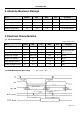
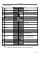
4.6 Basic Operating Sequence
4.6.1 Initialization Sequence
Code Function
A0
D7
D6
D5
D4
D
3
D2
D1
D0
hex
Note
Turn on Power Supply VDD & VSS While
maintaining /RES at LOW
- - - - - - - - - - -
Wait until power supply is stabilized - - - - - - - - - - -
Release the /RES Reset Signal
(/RES = High)
- - - - - - - - - -
See AC Characteristics section for timing
details
LCD Bias = 1/9 0 1 0 1 0 0 0 1 0 A2H LCD Characteristics
ADC = Normal 0 1 0 1 0 0 0 0 0 A0H No flip on x-direction (SEG)
SHL = Reverse 0 1 1 0 0 1 0 0 0 C8H Flip on y- direction (COM)
Initial Display Line = 0
0 0 1 0 0 0 0 0 0 40H
i.e. Display RAM “Page 0-D0”
Matched to top line of the LCD
Power Control
Voltage Follower = OFF
Voltage Regulator = OFF
Voltage Converter = ON
0 001011 00 2CH
Turn on the internal Voltage Converter and
wait until VOUT stable
Delay 50ms - - - - - - - - - -
Power Control
Voltage Follower = OFF
Voltage Regulator = OFF
Voltage Converter = ON
0 0 0 1 0 1 1 1 0 2EH
Turn on the internal Voltage Regulator and
wait until VOUT stable
Delay 50ms - - - - - - - - - -
Power Control
Voltage Follower = OFF
Voltage Regulator = OFF
Voltage Converter = ON
0 0 0 1 0 1 1 1 1 2FH
Turn on the internal Voltage Follower and
wait until VOUT stable
Delay 50ms - - - - - - - - - -
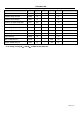
Regulator Resistor Select 0 0 0 1 0 0 1 0 1 25H Set the built-in resistor ratio to middle
Set Reference Voltage Mode 0 1 0 0 0 0 0 0 1 81H
Set Reference Voltage Resistor 0 0 0 1 0 0 0 0 0 20H
Set to the middle of the range it may be adjused
For achieving the best display contrast
Display ON 0 1 0 1 0 1 1 1 1 AFH Turn on the LCD display
Set Page Address = 0
0 101100 00 B0H
Specify the display data RAM page address to
00H
Set Column Address (Upper -4bit = 0) 0 0 0 0 1 0 0 0 0 10H
Set Column Address (Lower-4bit =4) 0 0 0 0 0 0 1 0 0 04H
Specify the display data RAM column address
to 00H
Write Display Data 1 Display Data -
Write Other Display Data
Page 11 of 14