
Data Sheet


Electrical specifications VNH5019A-E
14/37 Doc ID 15701 Rev 9
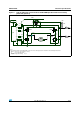
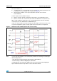
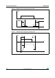
2.4 Waveforms and truth table
In normal operating conditions the DIAG
X
/EN
X
pin is considered as an input pin by the
device. This pin must be externally pulled-high
PWM pin usage: in all cases, a “0” on the PWM pin turns-off both LS
A
and LS
B
switches.
When PWM rises back to “1”, LS
A
or LS
B
turn-on again depending on the input pin state.
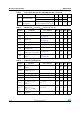
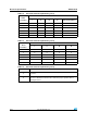
Table 11. Charge pump
Symbol Parameter Test conditions Min Typ Max Unit
V
CP
Charge pump output
voltage
EN
X
= 5 V V
CC
+ 5 V
CC
+ 10
V
EN
X
= 5 V, V
CC
= 4.5 V 10.5
I
BAT
Charge pump standby
current
EN
A
= EN
B
= 0 V 200 nA
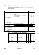
Table 12. Truth table in normal operating conditions
IN
A
IN
B
DIAG
A
/EN
A
DIAG
B
/EN
B
OUT
A
OUT
B
CS (V
CSD
= 0 V) Operating mode
1 1 1 1 H H High imp. Brake to V
CC
10 1 1 H LI
SENSE
= I
OUT
/K Clockwise (CW)
01 1 1 L HI
SENSE
= I
OUT
/K
Counterclockwise
(CCW)
0 0 1 1 L L High imp. Brake to GND