
Data Sheet


VNH5019A-E Electrical specifications
Doc ID 15701 Rev 9 13/37
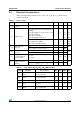
T
TSD_LS
Low-side thermal
shutdown temperature
V
IN
= 0 V 150 175 200 °C
T
TR
(3)
Thermal reset temperature 135 °C
T
HYST
(3)
Thermal hysteresis 7 15 °C
1. The device is able to pass the ESD and ISO pulse requirements as specified in the Table 15.
2. T
TSD
is the minimum threshold temperature between HS and LS
3. Valid for both HSD and LSD
Table 9. Protection and diagnostic (continued)
Symbol Parameter Test conditions Min Typ Max Unit
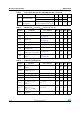
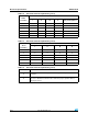
Table 10. Current sense (8 V < V
CC
< 21 V)
Symbol Parameter Test conditions Min Typ Max Unit
K
0
I
OUT
/I
SENSE
I
OUT
= 3 A, V
SENSE
= 0.5 V,
T
j
= - 40 °C to 150°C
4670 7110 10110
dK
0
/K
0
Analog current sense ratio
drift
I
OUT
= 3 A; V
SENSE
= 0.5 V,
T
j
= -40 °C to 150 °C
-19 19 %
K
1
I
OUT
/I
SENSE
I
OUT
= 8 A, V
SENSE
= 1.3V,
T
j
= - 40 °C to 150°C
6060 7030 8330
dK
1
/K
1
Analog current sense ratio
drift
I
OUT
= 8 A; V
SENSE
= 1.3V,
T
j
= -40 °C to 150 °C
-14 14 %
K
2
I
OUT
/I
SENSE
I
OUT
= 15 A, V
SENSE
= 2.4 V,
T
j
= - 40 °C to 150°C
6070 6990 7810
dK
2
/K
2
Analog current sense ratio
drift
I
OUT
= 15 A; V
SENSE
= 2.4 V,
T
j
= -40 °C to 150 °C
-12 12 %
K
3
I
OUT
/I
SENSE
I
OUT
= 25 A, V
SENSE
= 4 V,
T
j
= - 40 °C to 150°C
6000 6940 7650
dK
3
/K
3
Analog current sense ratio
drift
I
OUT
=25 A; V
SENSE
= 4 V,
T
j
= -40 °C to 150 °C
-12 12 %
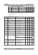
V
SENSE
Max analog sense output
voltage
I
OUT
= 15 A, R
SENSE
= 1.1 kΩ 5V
I
SENSEO
Analog sense leakage current
I
OUT
= 0 A, V
SENSE
= 0 V, V
CSD
= 5 V,
V
IN
= 0 V,
T
j
= - 40 to 150°C
05
µA
I
OUT
= 0 A, V
SENSE
= 0 V, V
CSD
= 0 V,
V
IN
= 5 V,
T
j
= - 40 to 150°C
0100
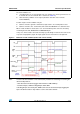
t
DSENSEH
Delay response time from
falling edge of CS_DIS pin
V
IN
= 5 V, V
SENSE
< 4 V, I
OUT
= 8 A,
I
SENSE
= 90% of I
SENSEmax
(see fig Figure 13)
50 µs
t
DSENSEL
Delay response time from
rising edge of CS_DIS pin
V
IN
= 5 V, V
SENSE
< 4 V, I
OUT
= 8 A,
I
SENSE
= 10% of I
SENSEmax
(see fig Figure 13)
20 µs