
Data Sheet

Analog Integrated Circuit Device Data
Freescale Semiconductor 7
33926
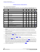
ELECTRICAL CHARACTERISTICS
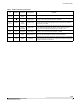
MAXIMUM RATINGS
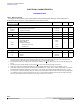
T
PPRT
Peak Package Reflow Temperature During Reflow
250
°C
(7)
(8)
R
JC
Approximate Junction-to-Case Thermal Resistance
< 1.0 C/W
(9)
Notes
7. Pin soldering temperature limit is for 10 seconds maximum duration. Not designed for immersion soldering. Exceeding these limits may
cause malfunction or permanent damage to the device.
8. Freescale’s Package Reflow capability meets Pb-free requirements for JEDEC standard J-STD-020C for Peak Package Reflow
Temperature and Moisture Sensitivity Levels (MSL),
9. Exposed heatsink pad plus the power and ground pins comprise the main heat conduction paths. The actual R
JB
(junction-to-PC board)
values will vary depending on solder thickness and composition and copper trace thickness and area. Maximum current at maximum die
temperature represents ~16
W of conduction loss heating in the diagonal pair of output MOSFETs. Therefore, the R
JA
must be
< 5.0 C/W for maximum current at 70 C ambient. Module thermal design must be planned accordingly.
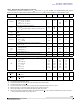
Table 3. Maximum Ratings (continued)
All voltages are with respect to ground unless otherwise noted. Exceeding these ratings may cause a malfunction or
permanent damage to the device. These parameters are not production tested.
Symbol Ratings Value Unit Notes