
Data Sheet

Analog Integrated Circuit Device Data
Freescale Semiconductor 5
33926
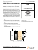
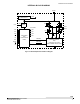
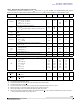
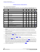
PIN CONNECTIONS
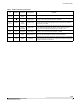
12, 13,
14, 15
OUT1
Power
Output
H-Bridge Output 1
Source of high-side MOSFET1 and drain of low-side MOSFET1.
16 D2 Logic Input
Disable Input 2
(Active Low)
When D2 is logic LOW, both OUT1 and OUT2 are tri-stated. (Schmitt trigger
input with ~80
A sink so default condition = disabled.)
18 – 20,
22
– 24
PGND
Power
Ground
Power Ground
High-current power ground pins must be connected together physically as
close as possible and directly soldered down to a wide, thick, low resistance
ground plane on the PCB.
21 SF
Logic
Output -
Open Drain
Status Flag
(Active Low)
Open drain active LOW status flag output (requires an external pull-up resistor
to
V
DD
. Maximum permissible load current < 0.5 mA. Maximum V
CESAT
<
0.4 V at 0.3 mA. Maximum permissible pull-up voltage < 7.0 V.)
26 D1 Logic Input
Disable Input 1
(Active High)
When D1 is logic HIGH, both OUT1 and OUT2 are tri-stated. Schmitt trigger
input with ~80
A source so default condition = disabled.
27, 28,
29, 30
OUT2
Power
Output
H-Bridge Output 2
Source of high-side MOSFET2 and drain of low-side MOSFET2.
32 CCP
Analog
Output
Charge Pump
Capacitor
External reservoir capacitor connection for internal charge pump; connected to
VPWR. Allowable values are 30 to 100
F. Note: This capacitor is required for
the proper performance of the device.
Table 2. 33926 Pin Definitions (continued)
Pin Pin Name
Pin
Function
Formal Name Definition