
Data Sheet

Analog Integrated Circuit Device Data
4 Freescale Semiconductor
33926
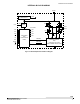
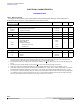
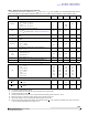
PIN CONNECTIONS
PIN CONNECTIONS
Figure 3. 33926 Pin Connections
A functional description of each pin can be found in the Functional Description section beginning on page 13.
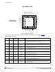
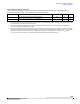
Table 2. 33926 Pin Definitions
Pin Pin Name
Pin
Function
Formal Name Definition
1 IN2 Logic Input Input 2
Logic input control of OUT2; e.g., when IN2 is logic HIGH, OUT2 is set to V
PWR
,
and when IN2 is logic LOW, OUT2 is set to PGND. (Schmitt trigger input with
~
80 A source so default condition = OUT2 HIGH.)
2 IN1 Logic Input Input 1
Logic input control of OUT1; e.g., when IN1 is logic HIGH, OUT1 is set to V
PWR
,
and when IN1 is logic LOW, OUT1 is set to PGND. (Schmitt trigger Input with
~
80 A source so default condition = OUT1 HIGH.)
3 SLEW Logic Input Slew Rate
Logic input to select fast or slow slew rate. (Schmitt trigger input with ~ 80 A
sink so default condition
= slow.)
4, 6, 11, 31 VPWR Power Input
Positive Power
Supply
These pins must be connected together physically as close as possible and
directly soldered down to a wide, thick, low resistance supply plane on the PCB.
5,
Exposed
Pad
AGND
Analog
Ground
Analog Signal
Ground
The low current analog signal ground must be connected to PGND via low
impedance path (<<10
m, 0 Hz to 20 kHz). Exposed copper pad is also the
main heatsinking path for the device.
7 INV Logic Input Input Invert
Sets IN1 and IN2 to logic LOW = TRUE. (Schmitt trigger input with ~ 80 A sink
so default condition
= non-inverted.)
8 FB
Analog
Output
Feedback
Load current feedback output provides ground referenced 0.24% of H-Bridge
high-side output current. (Tie pin to GND through a resistor if not used.)
9, 17, 25 NC No Connect
No internal connection is made to this pin.
10 EN Logic Input Enable Input
When EN is logic HIGH, the device is operational. When EN is logic LOW, the
device is placed in Sleep mode. (logic input with ~
80 A sink so default
condition = Sleep mode.)
Transparent Top
25
17
18
19
20
21
22
23
24
910111213141516
1
2
3
4
5
6
7
8
26272829303132
NC
NC
VPWR
NC
IN2
IN1
SLEW
OUT1
AGND
INV
FB
EN
OUT1
VPWR
VPWR
OUT2
OUT2
AGND
OUT1
D2
PGND
SF
D1
OUT2
OUT2
CCP
VPWR
PGND
PGND
PGND
PGND
PGND
OUT1
View of Package