
Data Sheet

Analog Integrated Circuit Device Data
18 Freescale Semiconductor
33926
FUNCTIONAL DEVICE OPERATION
PROTECTION AND DIAGNOSTIC FEATURES
PROTECTION AND DIAGNOSTIC FEATURES
SHORT-CIRCUIT PROTECTION
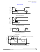
If an output short-circuit condition is detected, the power outputs tri-state (latch-OFF) independent of the input (IN1 and IN2)
states, and the fault status output flag (
SF) is SET to a logic LOW. If the D1 input changes from a logic HIGH to logic LOW, or if
the D2 input changes from a logic LOW to logic HIGH, the output bridge will become operational again, and the fault status flag
will be reset (cleared) to a logic HIGH state.
The output stage will always switch into the mode defined by the input pins (IN1, IN2, D1, and D2), provided the device junction
temperature is within the specified operating temperature range.
INTERNAL PWM CURRENT LIMITING
The maximum current flow under normal operating conditions should be less than 5.0 A. The instantaneous load currents will
be limited to I
LIM
via the internal PWM current limiting circuitry. When the I
LIM
threshold current value is reached, the output stages
are tri-stated for a fixed time (T
A
) of 20 µs typical. Depending on the time constant associated with the load characteristics, the
output current decreases during the tri-state duration until the next output ON cycle occurs.
The PWM current limit threshold value is dependent on the device junction temperature. When - 40 °C < T
J
< 160 °C, I
LIM
is
between the specified minimum/maximum values. When T
J
exceeds 160 °C, the I
LIM
threshold decreases to 4.2 A. Shortly above
175
°C the device overtemperature circuit will detect T
LIM
and an overtemperature shutdown will occur. This feature implements
a graceful degradation of operation before thermal shutdown occurs, thus allowing for intermittent unexpected mechanical loads
on the motor’s gear-reduction train to be handled.
Important Die temperature excursions above 150 C are permitted only for non-repetitive durations < 30 seconds. Provision
must be made at the system level to prevent prolonged operation in the current-foldback region.
OVERTEMPERATURE SHUTDOWN AND HYSTERESIS
If an overtemperature condition occurs, the power outputs are tri-stated (latched-OFF), and the fault status flag (SF) is SET to
a logic LOW.
To reset from this condition, D1 must change from a logic HIGH to logic LOW, or D2 must change from a logic LOW to logic
HIGH. When reset, the output stage switches ON again, provided that the junction temperature is now below the overtemperature
threshold limit minus the hysteresis.
Important Resetting from the fault condition will clear the fault status flag. Powering down and powering up the device will also
reset the 33926 from the fault condition.
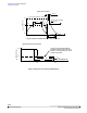
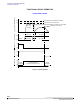
OUTPUT AVALANCHE PROTECTION
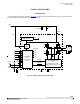
If VPWR were to become an open circuit, the outputs would likely tri-state simultaneously due to the disable logic. This could
result in an unclamped inductive discharge. The VPWR input to the 33926 should not exceed 40
V during this transient condition,
to prevent electrical overstress of the output drivers.This can be accomplished with a zener clamp or MOV, and/or an
appropriately valued input capacitor with sufficiently low ESR (see
Figure 13).
Figure 13. Avalanche Protection
OUT1
OUT2
I/Os
AGND PGND
Bulk
Low ESR
Cap.
VPWR
100nF
M
V
PWR
9